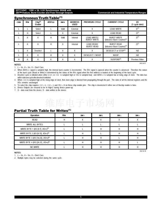
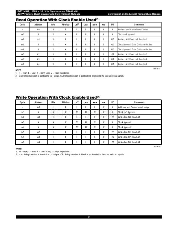
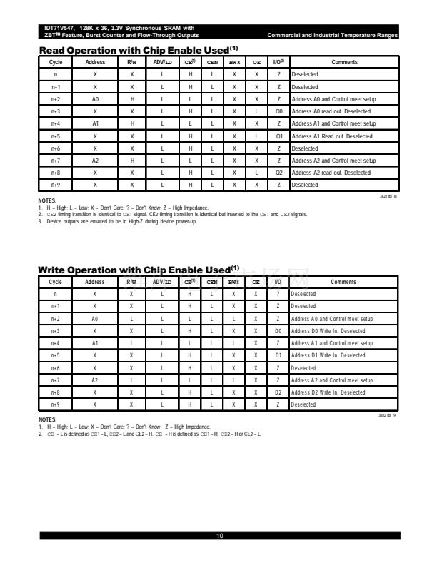
鈩?/div>
Commercial and Industrial Temperature Ranges
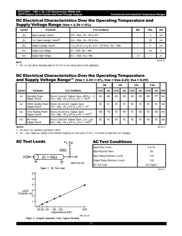
DC Electrical Characteristics Over the Operating Temperature and
Supply Voltage Range
(V
DD
= 3.3V +/-5%)
Symbol
|I
LI
|
|I
LI
|
|I
LO
|
V
OL
V
OH
Parameter
Input Leakage Current
LBO
Input Leakage Current
(1)
Output Leakage Current
Output Low Voltage
Output High Voltage
Test Conditions
V
DD
= Max., V
IN =
0V to V
DD
V
DD
= Max., V
IN =
0V to V
DD
CE
> V
IH
or
OE
> V
IH
, V
OUT
= 0V toV
DD
, V
DD
= Max.
I
OL
= 5mA, V
DD
= Min.
I
OH
= -5mA, V
DD
= Min.
Min.
___
Max.
5
30
5
0.4
___
Unit
碌A
碌A
碌A
V
V
3822 tbl 20
___
___
___
2.4
NOTE:
1. The
LBO
pin will be internally pulled to V
DD
if it is not actively driven in the application.
DC Electrical Characteristics Over the Operating Temperature
and Supply Voltage Range
(1)
(V
DD
= 3.3V +/-5%, V
HD
= V
DD
聳0.2V, V
LD
= 0.2V)
S80
Symbol
I
DD
I
SB1
I
SB2
I
SB3
Parameter
Operating Power
Supply Current
Test Conditions
Device Selected, Outputs Open, ADV/LD = X,
V
DD
= Max., V
IN
> V
IH
or < V
IL
, f = f
MAX
(2)
Com'l
250
40
100
40
Ind
260
45
110
45
S85
Com'l
225
40
95
40
Ind
235
45
105
45
S90
Com'l
225
40
95
40
Ind
235
45
105
45
S100
Com'l
200
40
90
40
Ind
210
45
100
45
Unit
mA
mA
mA
mA
3822 tbl 21
CMOS Standby Power Device Deselected, Outputs Open,
Supply Current
V
DD
= Max., V
IN
> V
HD
or < V
LD
, f = 0
(2)
Clock Running Power
Supply Current
Idle Power
Supply Current
Device Deselected, Outputs Open,
V
DD
= Max., V
IN
> V
HD
or < V
LD
, f = f
MAX
(2)
Device Selected, Outputs Open,
CEN
> V
IH
V
DD
= Max., V
IN
> V
HD
or < V
LD
, f = f
MAX
(2)
NOTES:
1. All values are maximum guaranteed values.
2. At f = f
MAX,
inputs are cycling at the maximum frequency of read cycles of 1/t
CYC
; f=0 means no input lines are changing.
AC Test Loads
+1.5V
50鈩?/div>
AC Test Conditions
Input Pulse Levels
Input Rise/Fall Times
Input Timing Reference Levels
Output Timing Reference Levels
AC Test Load
0 to 3V
2ns
1.5V
1.5V
See Figure 1
3822 tbl 22
I/O
Z
0
= 50鈩?/div>
3822 drw 04
Figure 1. AC Test Load
,
6
5
4
鈭唗CD
3
(Typical, ns)
2
1
20 30 50
80 100
Capacitance (pF)
200
3822 drw 05
.
11
6.42
Figure 2. Lumped Capacitive Load, Typical Derating


 1
1
 2
2
 3
3
 4
4
 5
5
 6
6
 7
7
 8
8
 9
9
 10
10
 11
11
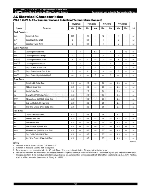 12
12
 13
13
 14
14
 15
15
 16
16
 17
17
 18
18
 19
19
