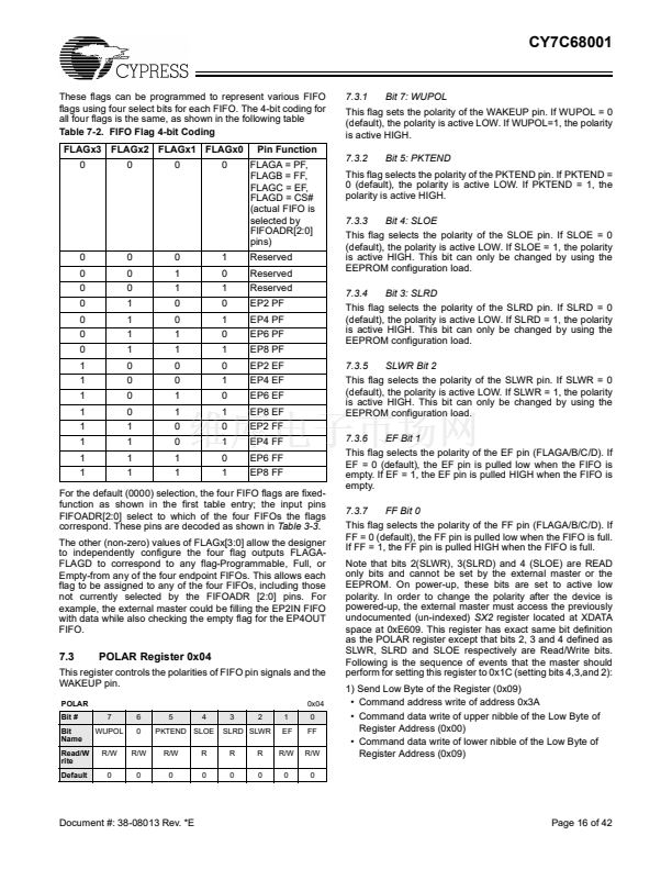
FOR
FOR
CY7C68001
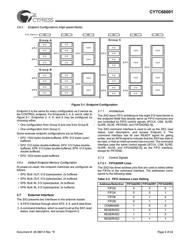
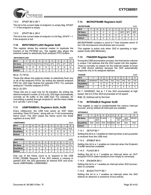
7.14.6
READY Bit 0
Setting this bit to a 1 enables an interrupt when the
SX2
has
powered on and performed an internal self-test.
to complete Endpoint 0 data transfers. For complete details,
refer to Section 5.0.
7.17
SETUP Register 0x32
7.15
DESC Register 0x30
This register address is used to write the 500-byte descriptor
RAM. The external master writes two bytes (four command
data transfers) to this address corresponding to the length of
the descriptor or VID/PID/DID data to be written. The external
master then consecutively writes that number of bytes into the
descriptor RAM in nibble format. For complete details, refer to
Section 4.0.
This register address is used to access the 8-byte set-up
packet received from the USB host. If the external master
writes to this register, it can stall Endpoint 0. For complete
details, refer to Section 5.0.
7.18
EP0BC Register 0x33
7.16
EP0BUF Register 0x31
This register address is used to access the 64-byte Endpoint
0 buffer. The external master can read or write to this register
This register address is used to access the byte count of
Endpoint 0. For Endpoint 0 OUT transfers, the external master
can read this register to get the number of bytes transferred
from the USB host. For Endpoint 0 IN transfers, the external
master writes the number of bytes in the Endpoint 0 buffer to
transfer the bytes to the USB host. For complete details, refer
to Section 5.0.
Document #: 38-08013 Rev. *E
Page 21 of 42


 1
1
 2
2
 3
3
 4
4
 5
5
 6
6
 7
7
 8
8
 9
9
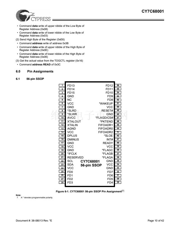 10
10
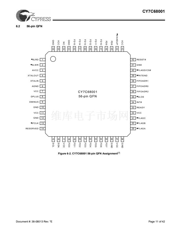 11
11
 12
12
 13
13
 14
14
 15
15
 16
16
 17
17
 18
18
 19
19
 20
20
 21
21
 22
22
 23
23
 24
24
 25
25
 26
26
 27
27
 28
28
 29
29
 30
30
 31
31
 32
32
 33
33
 34
34
 35
35
 36
36
 37
37
 38
38
 39
39
 40
40
 41
41
 42
42
 43
43
