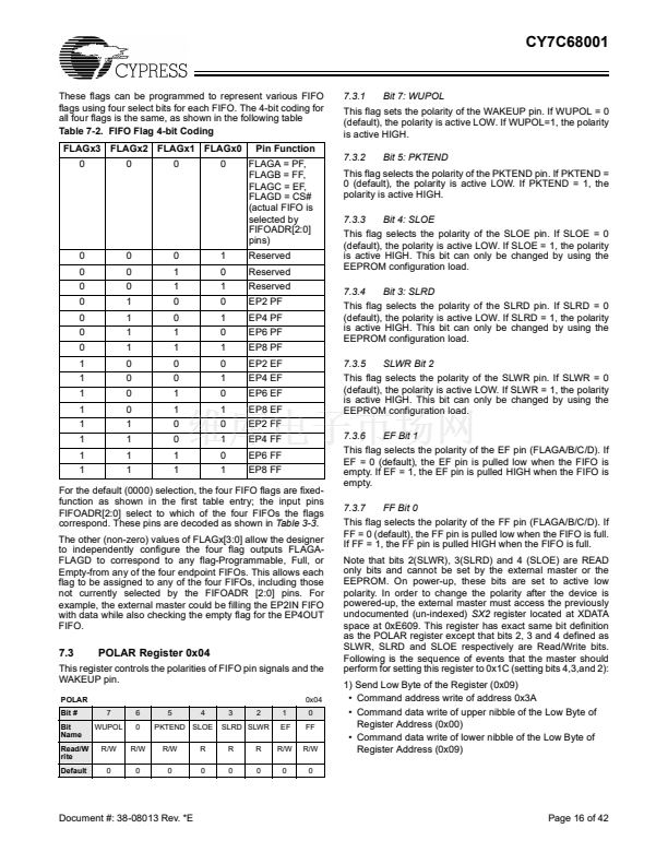
FOR
FOR
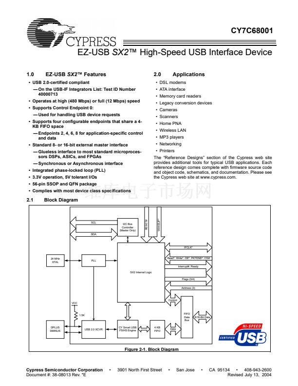
CY7C68001
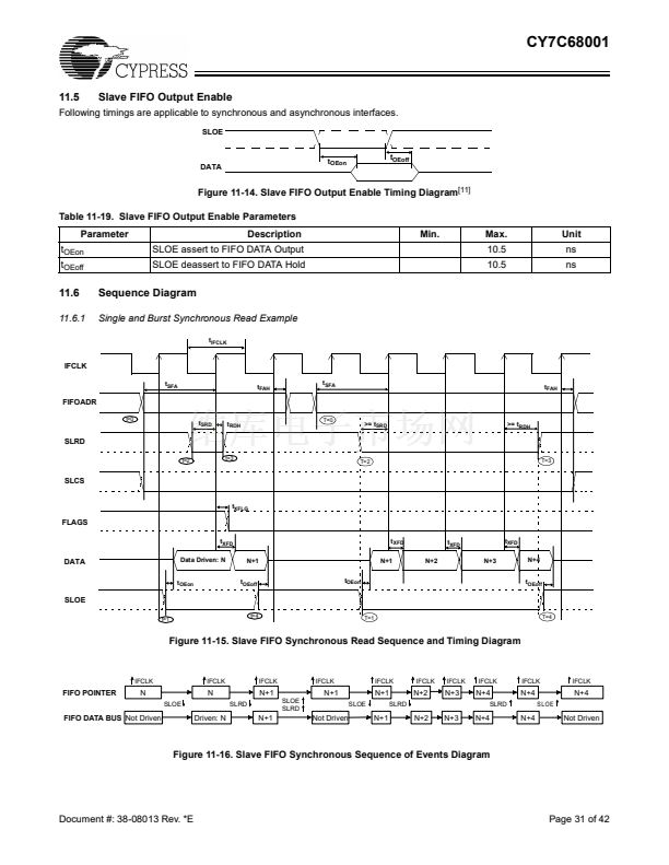
鈥?While the SLWR is asserted, data is written to the FIFO and
on the rising edge of the IFCLK, the FIFO pointer is incre-
mented. The FIFO flag will also be updated after a delay of
t
XFLG
from the rising edge of the clock.
The same sequence of events are also shown for a burst write
and are marked with the time indicators of T=0 through 5.
Note: For the burst mode, SLWR and SLCS are left asserted
for the entire duration of writing all the required data values. In
this burst write mode, once the SLWR is asserted, the data on
the FIFO data bus is written to the FIFO on every rising edge
of IFCLK. The FIFO pointer is updated on each rising edge of
IFCLK. In
Figure 11-17,
once the four bytes are written to the
FIFO, SLWR is de-asserted. The short 4-byte packet can be
committed to the host by asserting the PKTEND signal.
t
SFA
t
FAH
t
SFA
There is no specific timing requirement that needs to be met
for asserting PKTEND signal with regards to asserting the
SLWR signal. PKTEND can be asserted with the last data
value or thereafter. The only consideration is the setup time
t
SPE
and the hold time t
PEH
must be met. In the scenario of
Figure 11-17,
the number of data values committed includes
the last value written to the FIFO. In this example, both the
data value and the PKTEND signal are clocked on the same
rising edge of IFCLK. PKTEND can be asserted in subsequent
clock cycles. The FIFOADDR lines should be held constant
during the PKTEND assertion.
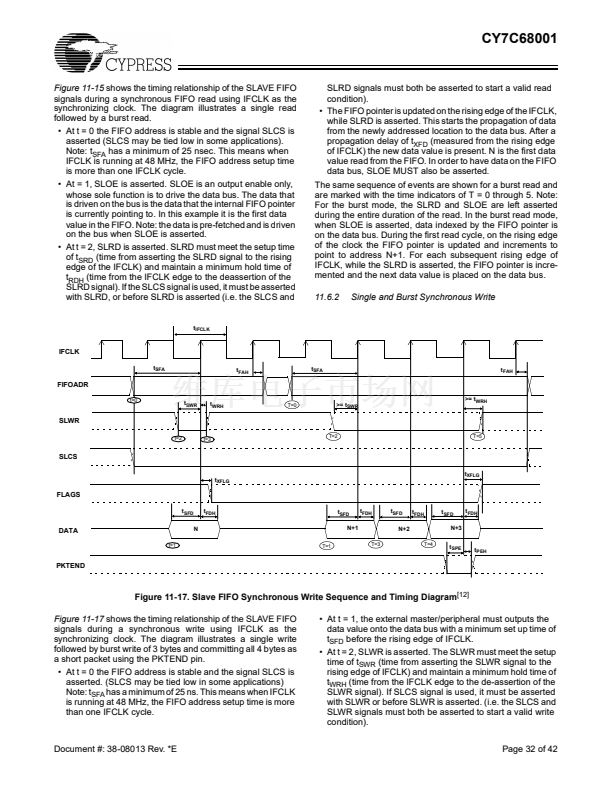
11.6.3 Sequence Diagram of a Single and Burst Asynchro-
nous Read
t
FAH
FIFOADR
t=0
t
RDpwl
t
RDpwh
T=0
t
RDpwl
t
RDpwh
t
RDpwl
t
RDpwh
t
RDpwl
t
RDpwh
SLRD
t=2
t=3
T=2
T=3
T=4
T=5
T=6
SLCS
t
XFLG
t
XFLG
FLAGS
t
XFD
t
XFD
N
t
OEoff
t
OEon
N+1
t
XFD
N+2
t
XFD
N+3
t
OEoff
DATA
Data (X)
Driven
t
OEon
N
SLOE
t=1
t=4
T=1
T=7
Figure 11-18. Slave FIFO Asynchronous Read Sequence and Timing Diagram
SLOE
SLRD
SLRD
SLOE
SLOE
SLRD
SLRD
SLRD
SLRD
SLOE
FIFO POINTER
N
N
Driven: X
N
N
N+1
N
N+1
Not Driven
N+1
N
N+1
N+1
N+2
N+1
N+2
N+2
N +3
N+2
N+3
Not Driven
FIFO DATA BUS
Not Driven
Figure 11-19. Slave FIFO Asynchronous Read Sequence of Events Diagram
Figure 11-18
diagrams the timing relationship of the SLAVE
FIFO signals during an asynchronous FIFO read. It shows a
single read followed by a burst read.
鈥?At t = 0 the FIFO address is stable and the SLCS signal is
asserted.
鈥?At t = 1, SLOE is asserted. This results in the data bus being
driven. The data that is driven on to the bus is previous data,
it data that was in the FIFO from a prior read cycle.
鈥?At t = 2, SLRD is asserted. The SLRD must meet the
minimum active pulse of t
RDpwl
and minimum de-active
pulse width of t
RDpwh
. If SLCS is used then, SLCS must be
in asserted with SLRD or before SLRD is asserted. (i.e. the
SLCS and SLRD signals must both be asserted to start a
valid read condition.)
鈥?The data that will be driven, after asserting SLRD, is the
updated data from the FIFO. This data is valid after a propa-
gation delay of t
XFD
from the activating edge of SLRD. In
Figure 11-18,
data N is the first valid data read from the
FIFO. For data to appear on the data bus during the read
cycle (i.e. SLRD is asserted), SLOE MUST be in an asserted
state. SLRD and SLOE can also be tied together.
The same sequence of events is also shown for a burst read
marked with T = 0 through 5. Note: In burst read mode, during
SLOE is assertion, the data bus is in a driven state and outputs
the previous data. Once SLRD is asserted, the data from the
Document #: 38-08013 Rev. *E
Page 33 of 42


 1
1
 2
2
 3
3
 4
4
 5
5
 6
6
 7
7
 8
8
 9
9
 10
10
 11
11
 12
12
 13
13
 14
14
 15
15
 16
16
 17
17
 18
18
 19
19
 20
20
 21
21
 22
22
 23
23
 24
24
 25
25
 26
26
 27
27
 28
28
 29
29
 30
30
 31
31
 32
32
 33
33
 34
34
 35
35
 36
36
 37
37
 38
38
 39
39
 40
40
 41
41
 42
42
 43
43
