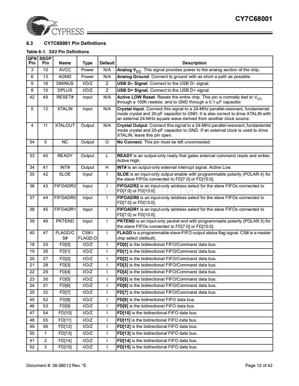
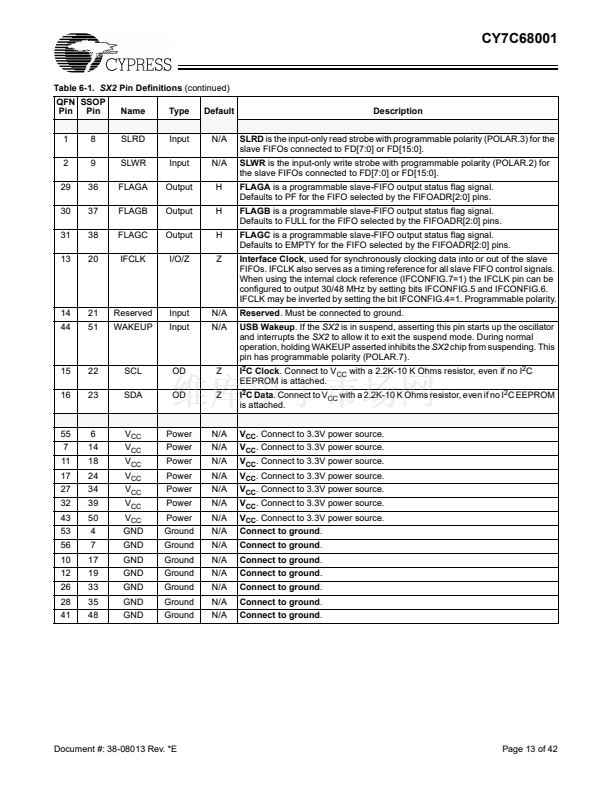
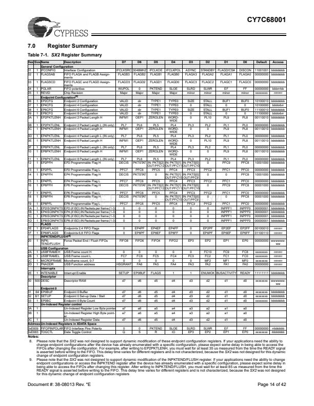
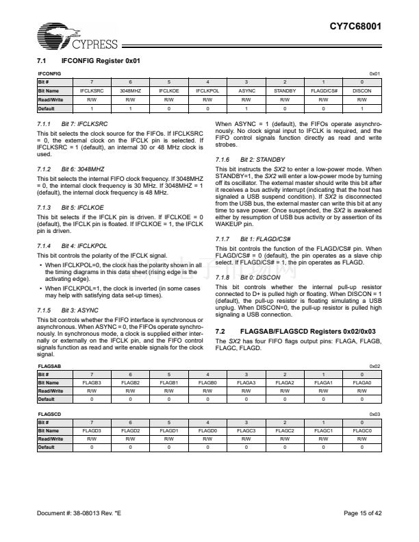
FOR
FOR
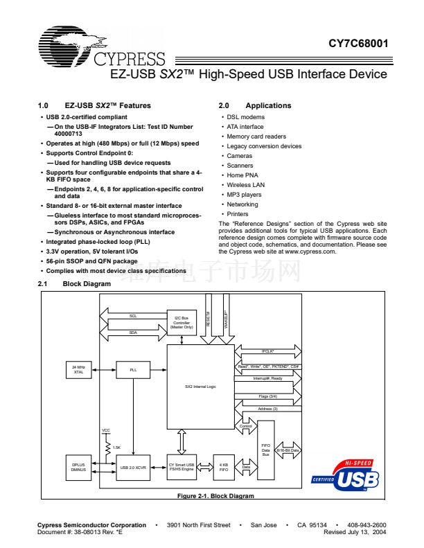
CY7C68001
3.7.8
Command Protocol
An address of [1 0 0] on FIFOADR [2:0] will select the
command interface. The command interface is used to write
to and read from the
SX2
registers and the Endpoint 0 buffer,
as well as the descriptor RAM. Command read and write trans-
actions occur over FD[7:0] only. Each byte written to the
SX2
is either an address or a data byte, as determined by bit7. If
bit7 = 1, then the byte is considered an address byte. If bit7 =
0, then the byte is considered a data byte. If bit7 = 1, then bit6
determines whether the address byte is a read request or a
write request. If bit6 = 1, then the byte is considered a read
request. If bit6 = 0 then the byte is considered a write request.
Bits [5:0] hold the register address of the request. The format
of the command address byte is shown in
Table 3-4.
Table 3-4. Command Address Byte
Address/
Data#
Read/
Write#
A5
A4
A3
A2
A1
A0
鈥?The next six bits represent the register address (000001
binary = 0x01 hex).
Once the byte has been received the
SX2
pulls the READY
pin low to inform the external master not to send any more
information. When the
SX2
is ready to receive the next byte,
the
SX2
pulls the READY pin high again. This next byte, the
upper nibble of the data byte, is written to the
SX2
as follows.
Table 3-8. Command Data Write Byte One
Address/
Data#
0
Don鈥檛
Care
X
Don鈥檛
Care
X
Don鈥檛
Care
X
D7
1
D6
0
D5
1
D4
1
鈥?The first bit signifies that this is a data transfer.
鈥?The next three are don鈥檛 care bits.
鈥?The next four bits hold the upper nibble of the transferred
byte.
Once the byte has been received the
SX2
pulls the READY
pin low to inform the external master not to send any more
information. When the
SX2
is ready to receive the next byte,
the
SX2
pulls the READY pin high again. This next byte, the
lower nibble of the data byte is written to the
SX2.
Table 3-9. Command Data Write Byte Two
Address/
Data#
0
Don鈥檛
Care
X
Don鈥檛
Care
X
Don鈥檛
Care
X
D3
0
D2
0
D1
0
D0
0
Bit 7
Bit 6
Bit 5
Bit 4
Bit 3
Bit 2
Bit 1
Bit 0
Each Write request is followed by two or more data bytes. If
another address byte is received before both data bytes are
received, the
SX2
ignores the first address and any incomplete
data transfers. The format for the data bytes is shown in
Table 3-5
and
Table 3-6.
Some registers take a series of bytes.
Each byte is transferred using the same protocol.
Table 3-5. Command Data Byte One
Bit 7
0
Bit 6
X
Bit 5
X
Bit 4
X
Bit 3
D7
Bit 2
D6
Bit 1
D5
Bit 0
D4
At this point the entire byte <10110000> has been transferred
to register 0x01 and the write sequence is complete.
3.7.8.2 Read Request Example
Table 3-6. Command Data Byte Two
Bit 7
0
Bit 6
X
Bit 5
X
Bit 4
X
Bit 3
D3
Bit 2
D2
Bit 1
D1
Bit 0
D0
The first command data byte contains the upper nibble of data,
and the second command byte contains the lower nibble of
data.
3.7.8.1 Write Request Example
Prior to writing to a register, two conditions must be met:
FIFOADR[2:0] must hold [1 0 0], and the Ready line must be
HIGH. The external master should not initiate a command if
the READY pin is not in a HIgh state.
Example:
to write the byte <10110000> into the IFCONFIG
register (0x01), first send a command address byte as follows.
Table 3-7. Command Address Write Byte
Address/ Read/
Data#
Write#
1
0
A5
0
A4
0
A3
0
A2
0
A1
0
A0
1
The Read cycle is simpler than the write cycle. The Read cycle
consists of a read request from the external master to the
SX2.
For example, to read the contents of register 0x01, a
command address byte is written to the
SX2
as follows.
Table 3-10. Command Address Read Byte
Address/ Read/
Data#
Write#
1
1
A5
0
A4
0
A3
0
A2
0
A1
0
A0
1
When the data is ready to be read, the
SX2
asserts the INT#
pin to tell the external master that the data it requested is
waiting on FD[7:0].
[5]
鈥?The first bit signifies an address transfer.
鈥?The second bit signifies that this is a write command.
Note:
4. In indexed mode, the value of the FLAGx pins is indeterminate except when addressing a FIFO (FIFOADR[2:0]={000,001,010,011}).
5. An important note: Once the
SX2
receives a Read request, the
SX2
allocates the interrupt line solely for the read request. If one of the six interrupt sources
described in Section 3.4 is asserted, the
SX2
will buffer that interrupt until the read request completes.
Document #: 38-08013 Rev. *E
Page 7 of 42


 1
1
 2
2
 3
3
 4
4
 5
5
 6
6
 7
7
 8
8
 9
9
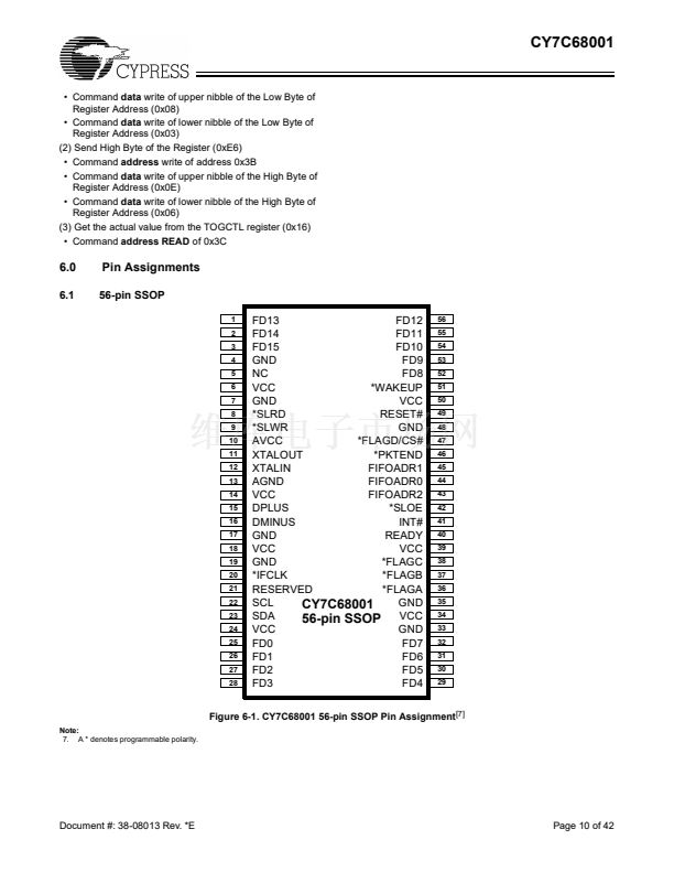 10
10
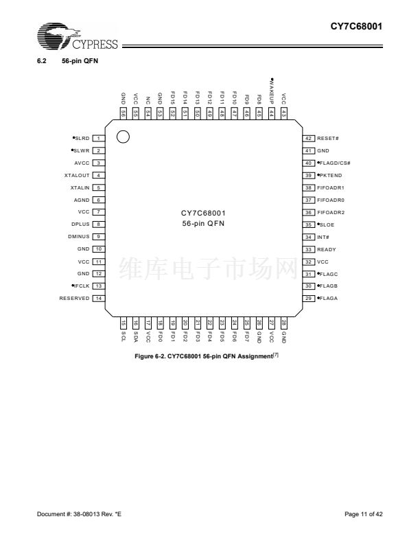 11
11
 12
12
 13
13
 14
14
 15
15
 16
16
 17
17
 18
18
 19
19
 20
20
 21
21
 22
22
 23
23
 24
24
 25
25
 26
26
 27
27
 28
28
 29
29
 30
30
 31
31
 32
32
 33
33
 34
34
 35
35
 36
36
 37
37
 38
38
 39
39
 40
40
 41
41
 42
42
 43
43
