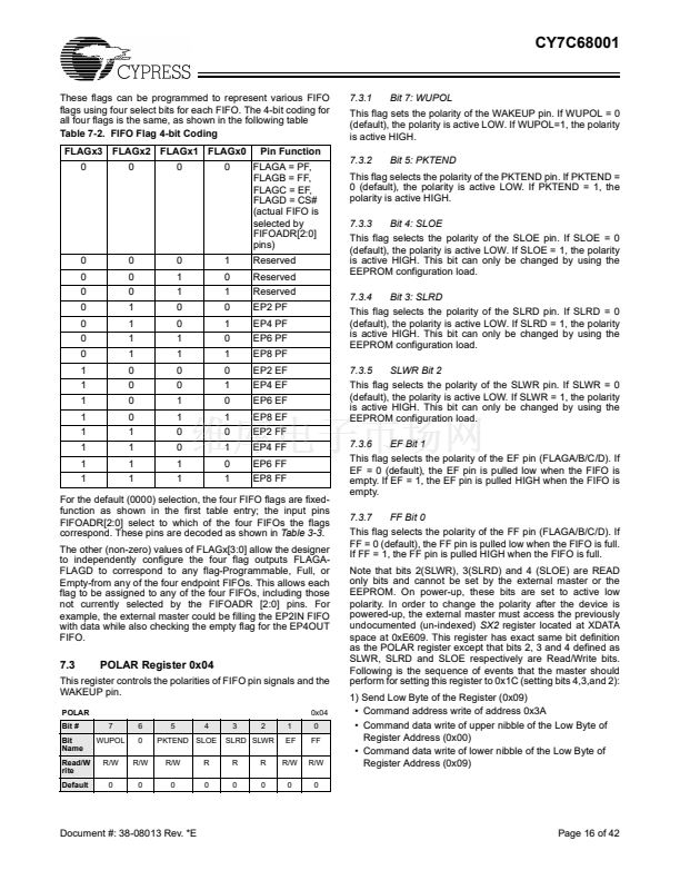
FOR
FOR
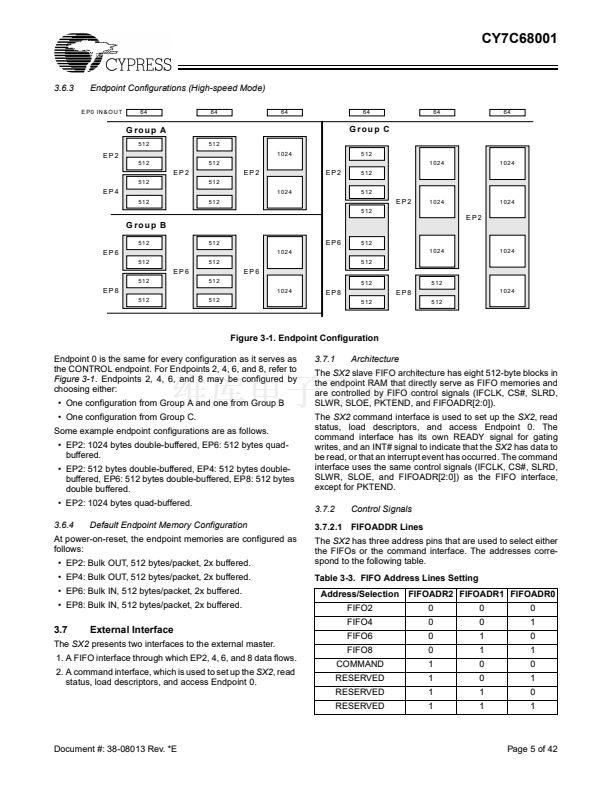
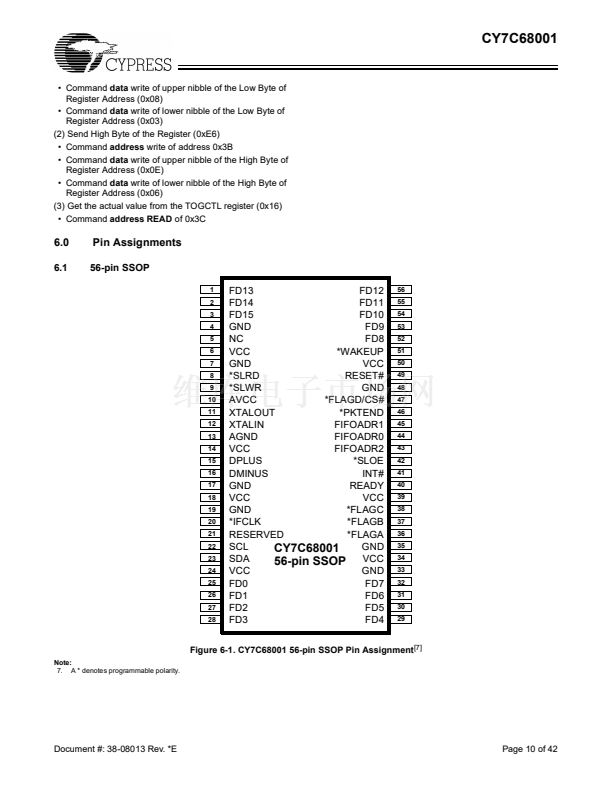
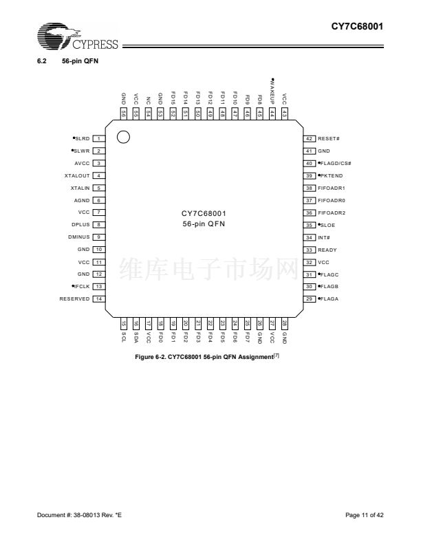
CY7C68001
For an OUT set-up transaction, the external master can read
each packet received from the USB host during the data
phase. The steps to read a packet are as follows:
1. Wait for an EP0BUF interrupt, indicating that a packet was
received from the USB host into the buffer.
2. Initiate a read request for the byte count register, 0x33.
This indicates the amount of data received from the host.
3. Initiate a read request for register 0x31.
4. Read one byte.
5. Repeat steps 3 and 4 until the number of bytes specified
in the byte count register has been read.
To receive more than 64 bytes, the process is repeated. The
SX2
internally stores the length of the data phase that was
specified in the wLength field of the set-up packet (bytes 6,7).
When the
SX2
sees that the specified number of bytes have
been received, it will complete the set-up transfer by automat-
ically completing the handshake phase. If the external master
does not wish to receive the entire transfer, it can stall the
transfer.
If the
SX2
receives another set-up packet before the current
transfer has completed, it will interrupt the external master with
another SETUP interrupt. If the
SX2
receives a set-up packet
with no data phase, the external master can accept the packet
and complete the handshake phase by writing zero to the byte
count register.
The
SX2
automatically responds to all USB standard requests
covered in chapter 9 of the USB 2.0 specification except the
Set/Clear Feature Endpoint requests. When the host issues a
Set Feature or a Clear feature request, the
SX2
will trigger a
SETUP interrupt to the external master. The USB spec
requires that the device respond to the Set endpoint feature
request by doing the following:
鈥?Set the STALL condition on that endpoint.
The USB spec requires that the device respond to the Clear
endpoint feature request by doing the following:
鈥?Reset the Data Toggle for that endpoint
鈥?Clear the STALL condition of that endpoint.
The register that is used to reset the data toggle TOGCTL
(located at XDATA location 0xE683) is not an index register
that can be addressed by the command protocol presented in
Section 3.7.8. The following section provides further infor-
mation on this register bits and how to reset the data toggle
accordingly using a different set of command protocol
sequence.
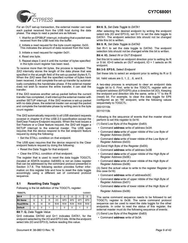
Bit 6: S,
Set Data Toggle to DATA1
After selecting the desired endpoint by writing the endpoint
select bits (IO and EP3:0), set S=1 to set the data toggle to
DATA1. The endpoint selection bits should not be changed
while this bit is written.
Bit 5: R,
Set Data Toggle to DATA0
Set R=1 to set the data toggle to DATA0. The endpoint
selection bits should not be changed while this bit is written.
Bit 4: IO,
Select IN or OUT Endpoint
Set this bit to select an endpoint direction prior to setting its R
or S bit. IO=0 selects an OUT endpoint, IO = 1 selects an IN
endpoint.
Bit 3-0: EP3:0,
Select Endpoint
Set these bits to select an endpoint prior to setting its R or S
bit. Valid values are 0, 1, 2, , 6, and 8.
A two-step process is employed to clear an endpoint data
toggle bit to 0. First, write to the TOGCTL register with an
endpoint address (EP3:EP0) plus a direction bit (IO). Keeping
the endpoint and direction bits the same, write a 鈥?鈥?to the R
(reset) bit. For example, to clear the data toggle for EP6
configured as an 鈥淚N鈥?endpoint, write the following values
sequentially to TOGCTL:
00010110b
00110110b
Following is the sequence of events that the master should
perform to set this register to 0x16:
(1) Send Low Byte of the Register (0x83)
鈥?Command
address
write of address 0x3A
鈥?Command
data
write of upper nibble of the Low Byte of
Register Address (0x08)
鈥?Command
data
write of lower nibble of the Low Byte of
Register Address (0x03)
(2) Send High Byte of the Register (0xE6)
鈥?Command
address
write of address 0x3B
鈥?Command
data
write of upper nibble of the High Byte of
Register Address (0x0E)
鈥?Command
data
write of lower nibble of the High Byte of
Register Address (0x06)
(3) Send the actual value to write to the register Register (in
this case 0x16)
鈥?Command
address
write of address0x3C
鈥?Command
data
write of upper nibble of the High Byte of
Register Address (0x01)
鈥?Command
data
write of lower nibble of the High Byte of
Register Address (0x06)
The same command sequence needs to be followed to set
TOGCTL register to 0x36. The same command protocol
sequence can be used to reset the data toggle for the other
endpoints. In order to read the status of this register, the
external master must do the following sequence of events:
(1) Send Low Byte of the Register (0x83)
鈥?Command
address
write of 0x3A
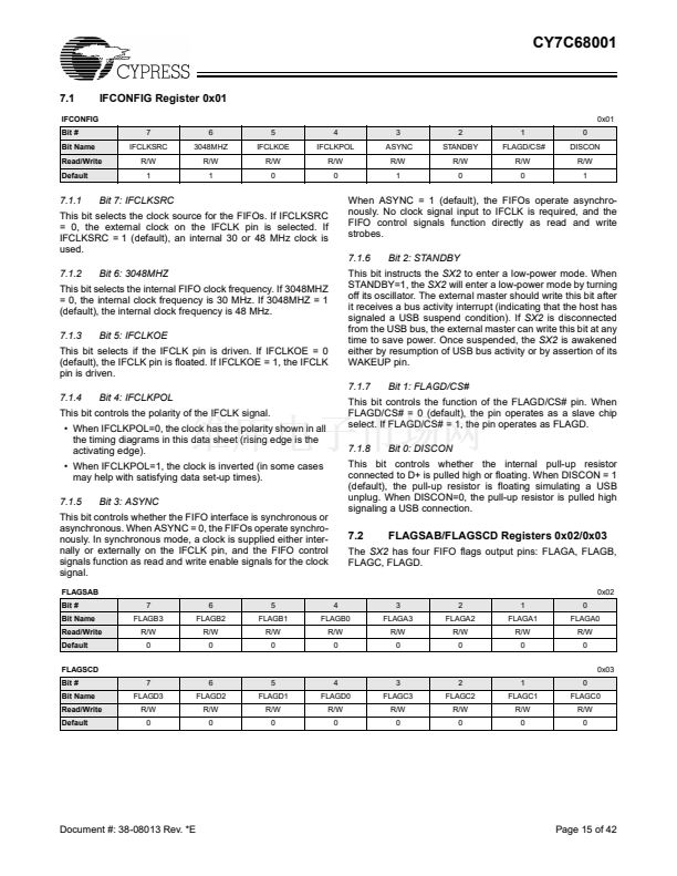
5.1
TOGCTL
Bit #
Bit Name
Resetting Data Toggle
0xE683
7
Q
R
0
6
S
W
0
5
R
W
1
4
I/O
R/W
1
3
EP3
R/W
0
2
EP2
R/W
0
1
EP1
R/W
1
0
EP0
R/W
0
Following is the bit definition of the TOGCTL register:
Read/Write
Default
Bit 7: Q,
Data Toggle Value
Q=0 indicates DATA0 and Q=1 indicates DATA1, for the
endpoint selected by the I/O and EP3:0 bits. Write the endpoint
select bits (IO and EP3:0), before reading this value.
Document #: 38-08013 Rev. *E
Page 9 of 42


 1
1
 2
2
 3
3
 4
4
 5
5
 6
6
 7
7
 8
8
 9
9
 10
10
 11
11
 12
12
 13
13
 14
14
 15
15
 16
16
 17
17
 18
18
 19
19
 20
20
 21
21
 22
22
 23
23
 24
24
 25
25
 26
26
 27
27
 28
28
 29
29
 30
30
 31
31
 32
32
 33
33
 34
34
 35
35
 36
36
 37
37
 38
38
 39
39
 40
40
 41
41
 42
42
 43
43
