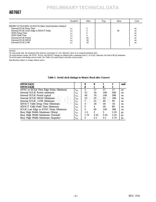
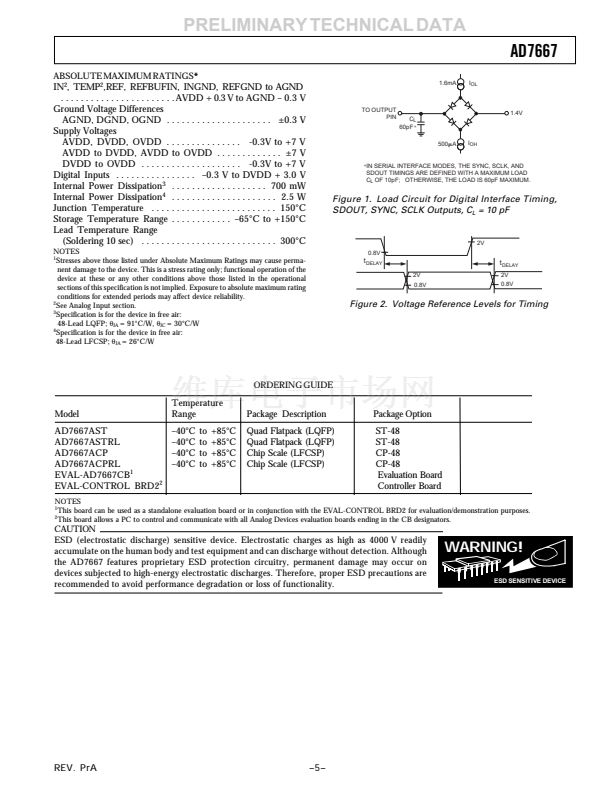
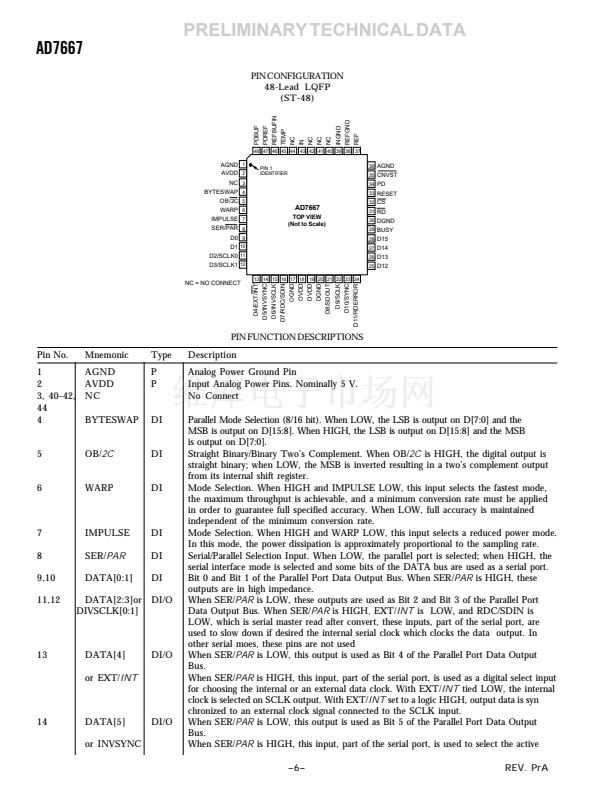
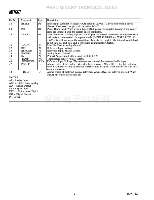
PRELIMINARY TECHNICAL DATA
AD7667
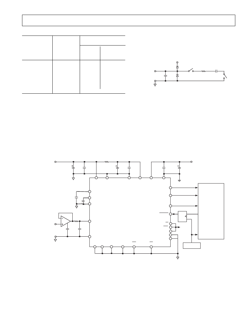
Table I. Output Codes and Ideal Input Voltages
Digital Output Code
Hexa
Straight Two鈥檚
Binary
Comple-
FFFF
FFFE
8001
8000
7FFF
0001
0000
2
1
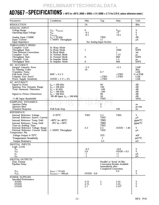
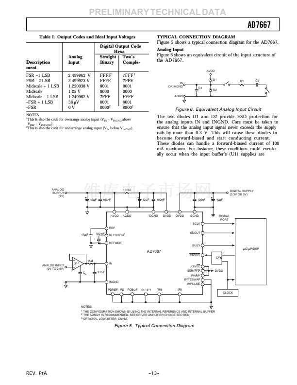
TYPICAL CONNECTION DIAGRAM
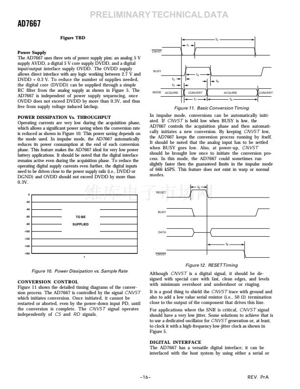
Figure 5 shows a typical connection diagram for the AD7667.
Analog Input
D
escription
ment
FSR 鈥? LSB
FSR 鈥?2 LSB
Midscale + 1 LSB
Midscale
Midscale 鈥?1 LSB
鈥揊SR + 1 LSB
鈥揊SR
Analog
Input
2.499962 V
2.499923 V
1.250038 V
1.25 V
1.249962 V
38 碌V
0V
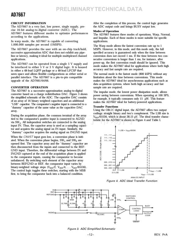
Figure 6 shows an equivalent circuit of the input structure of
the AD7667.
AVDD
7FFF
7FFE
0001
0000
FFFF
8001
8000
2
1
D1
IN
OR INGND
AGND
C1
R1
C2
D2
Figure 6. Equivalent Analog Input Circuit
NOTES
1
This is also the code for overrange analog input (V
IN
鈥?V
INGND
above
V
REF
鈥?V
REFGND
).
2
This is also the code for underrange analog input (V
IN
below V
INGND
).
The two diodes D1 and D2 provide ESD protection for
the analog inputs IN and INGND. Care must be taken to
ensure that the analog input signal never exceeds the supply
rails by more than 0.3 V. This will cause these diodes to
become forward-biased and start conducting current.
These diodes can handle a forward-biased current of 100
mA maximum. For instance, these conditions could eventu-
ally occur when the input buffer鈥檚 (U1) supplies are
ANALOG
SUPPLY
(5V)
10 F
100nF
100
10 F
100nF
100nF
10 F
DIGITAL SUPPLY
(3.3V OR 5V)
AVDD
AGND
DGND
DVDD
OVDD
OGND
SCLK
SERIAL
PORT
REF
47 F
100 nF
REFBUFIN1
REFGND
SDOUT
BUSY
AD7667
CNVST
U1
2
C
C
15
IN
2.7nF
INGND
PDREF PD
PDBUF
RESET
CS
RD
OB/ 2C
SER/ PAR
WARP
BYTESWAP
IMPULSE
CLOCK
DVDD
D
3
C/ P/DSP
ANALOG INPUT
(0V TO 2.5V)
NOTES:
1
2
THE CONFIGURATION SHOWN IS USING THE INTERNAL REFERENCE AND INTERNAL BUFFER
THE AD8021 IS RECOMMENDED. SEE DRIVER AMPLIFIER CHOICE SECTION.
3
OPTIONAL LOW JITTER CNVST.
Figure 5. Typical Connection Diagram
REV. PrA
鈥?3鈥?/div>
prev
next


 1
1
 2
2
 3
3
 4
4
 5
5
 6
6
 7
7
 8
8
 9
9
 10
10
 11
11
 12
12
 13
13
 14
14
 15
15
 16
16
 17
17
 18
18
 19
19
 20
20
 21
21
 22
22
 23
23
