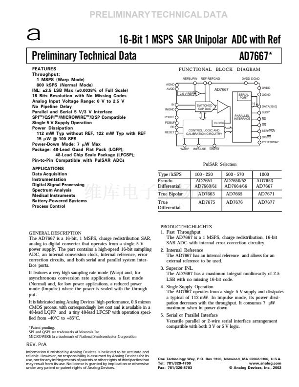
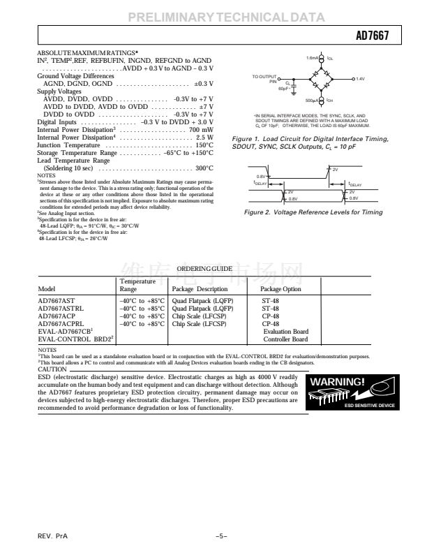
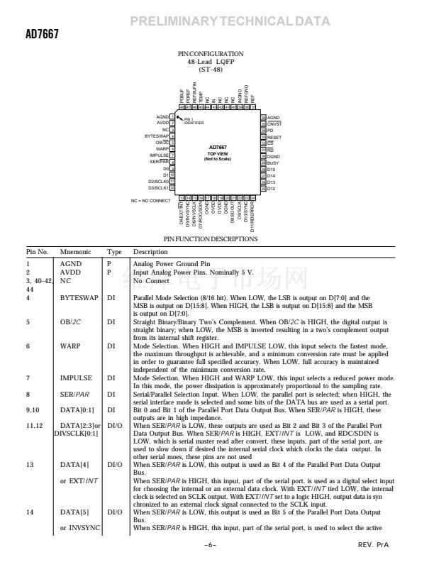
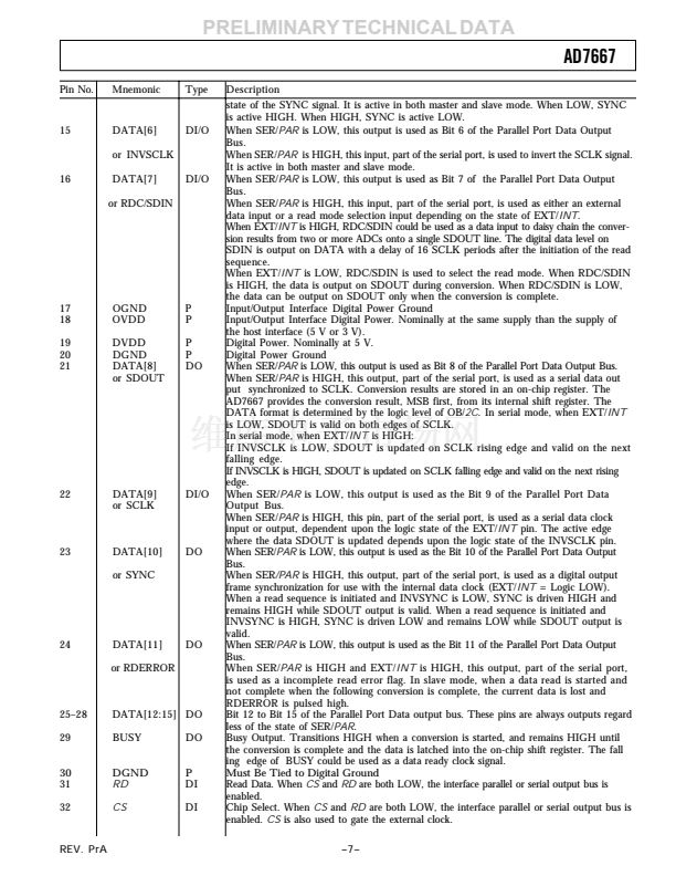
PRELIMINARY TECHNICAL DATA
AD7667
Figure TBD
t
1
t
2
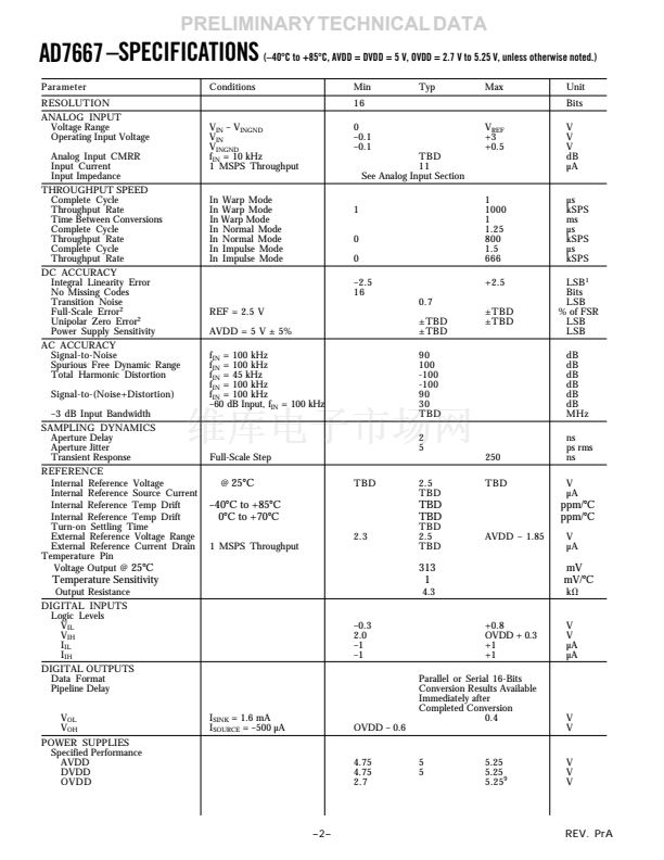
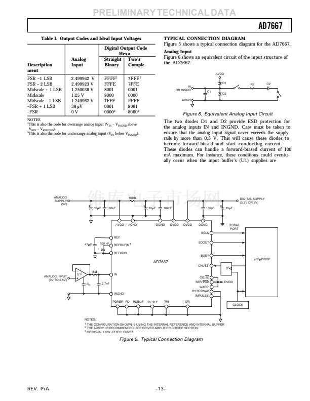
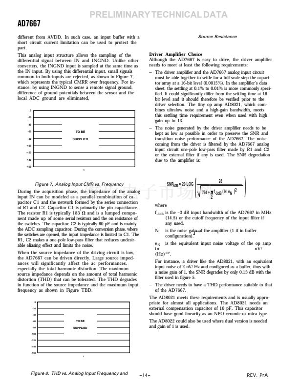
Power Supply
CNVST
The AD7667 uses three sets of power supply pins: an analog 5 V
supply AVDD, a digital 5 V core supply DVDD, and a digital
input/output interface supply OVDD. The OVDD supply
allows direct interface with any logic working between 2.7 V and
DVDD + 0.3 V. To reduce the number of supplies needed,
the digital core (DVDD) can be supplied through a simple
RC filter from the analog supply as shown in Figure 5. The
AD7667 is independent of power supply sequencing, once
OVDD does not exceed DVDD by more than 0.3V, and thus
free from supply voltage induced latchup.
POWER DISSIPATION Vs. THROUGHPUT
BUSY
t
4
t
3
t
5
MODE
ACQUIRE
CONVERT
t
6
ACQUIRE
CONVERT
t
7
t
8
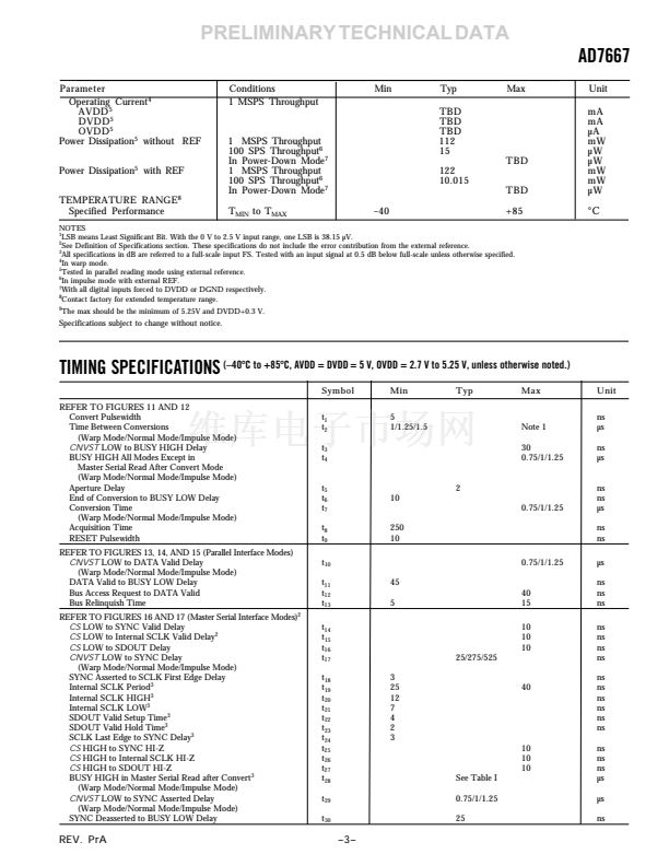
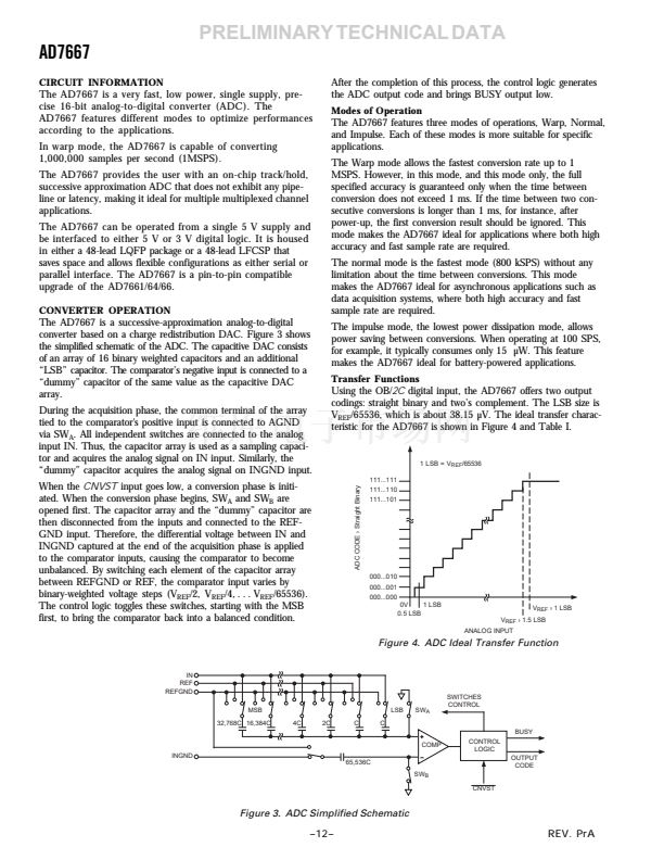
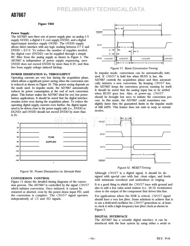
Figure 11. Basic Conversion Timing
Operating currents are very low during the acquisition phase,
which allows a significant power saving when the conversion rate
is reduced as shown in Figure 10. This power saving depends on
the mode used. In impulse mode, the AD7667 automatically
reduces its power consumption at the end of each conversion
phase. This feature makes the AD7667 ideal for very low power
battery applications. It should be noted that the digital interface
remains active even during the acquisition phase. To reduce the
operating digital supply currents even further, the digital inputs
need to be driven close to the power supply rails (i.e., DVDD or
DGND) and OVDD should not exceed DVDD by more than
0.3V.
0
-20
-40
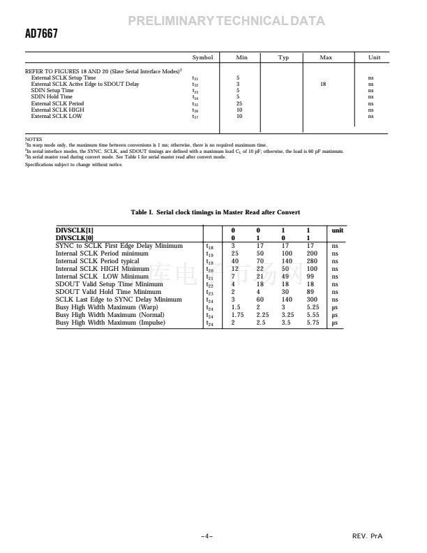
In impulse mode, conversions can be automatically initi-
ated. If
CNVST
is held low when BUSY is low, the
AD7667 controls the acquisition phase and then automati-
cally initiates a new conversion. By keeping
CNVST
low,
the AD7667 keeps the conversion process running by itself.
It should be noted that the analog input has to be settled
when BUSY goes low. Also, at power-up,
CNVST
should be brought low once to initiate the conversion pro-
cess. In this mode, the AD7667 could sometimes run
slightly faster then the guaranteed limits in the impulse mode
of 666 kSPS. This feature does not exist in warp or normal
modes.
t
9
RESET
BUSY
-60
-80
-100
-120
-140
-160
1
TO BE
SUPPLIED
DATA
t
8
CNVST
Figure 12. RESET Timing
Figure 10. Power Dissipation vs. Sample Rate
CONVERSION CONTROL
Figure 11 shows the detailed timing diagrams of the conver-
sion process. The AD7667 is controlled by the signal
CNVST
which initiates conversion. Once initiated, it cannot be
restarted or aborted, even by the power-down input PD, until
the conversion is complete. The
CNVST
signal operates
independently of
CS
and
RD
signals.
Although
CNVST
is a digital signal, it should be de-
signed with special care with fast, clean edges, and levels
with minimum overshoot and undershoot or ringing.
It is a good thing to shield the
CNVST
trace with ground and
also to add a low value serial resistor (i.e., 50 ) termination
close to the output of the component that drives this line.
For applications where the SNR is critical,
CNVST
signal
should have a very low jitter. Some solutions to achieve that is
to use a dedicated oscillator for
CNVST
generation or, at least,
to clock it with a high-frequency low-jitter clock as shown in
Figure 5.
DIGITAL INTERFACE
The AD7667 has a versatile digital interface; it can be
interfaced with the host system by using either a serial or
prev
next


 1
1
 2
2
 3
3
 4
4
 5
5
 6
6
 7
7
 8
8
 9
9
 10
10
 11
11
 12
12
 13
13
 14
14
 15
15
 16
16
 17
17
 18
18
 19
19
 20
20
 21
21
 22
22
 23
23
