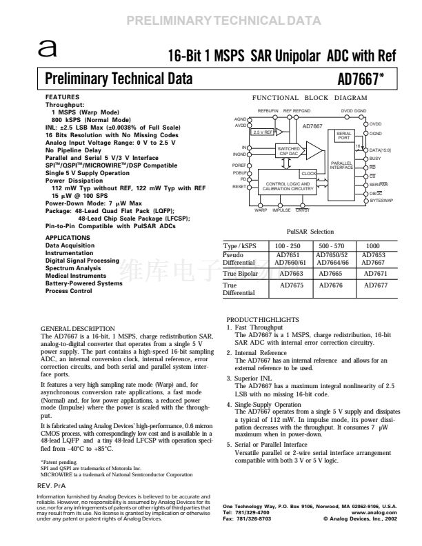
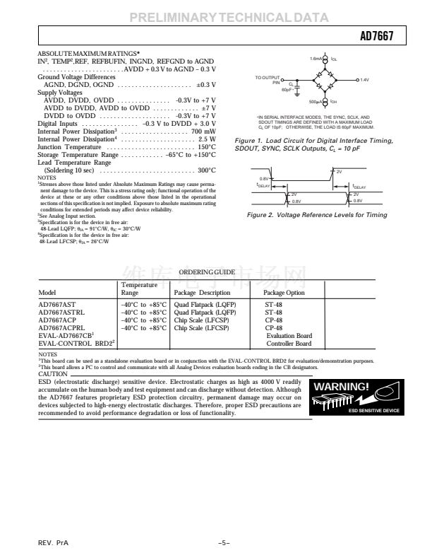
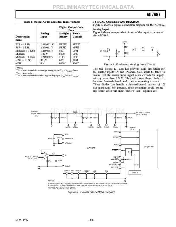
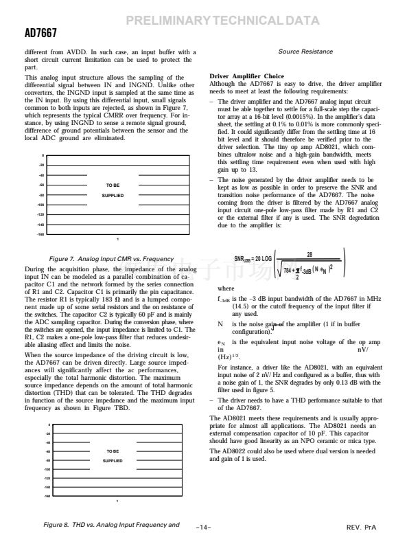
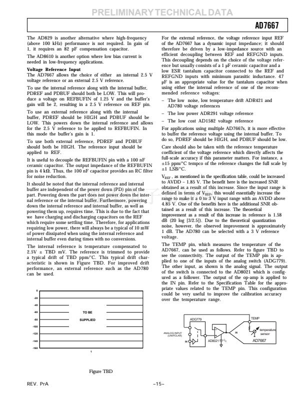
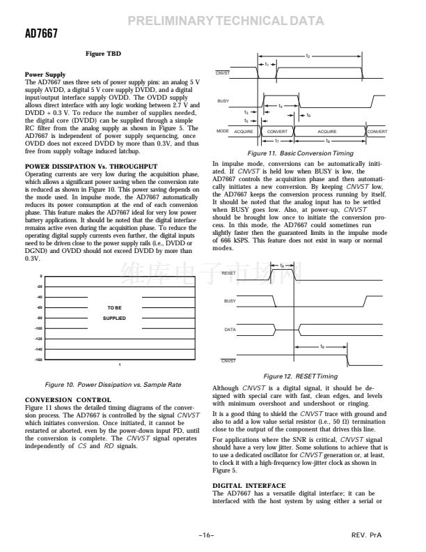
PRELIMINARY TECHNICAL DATA
AD7667
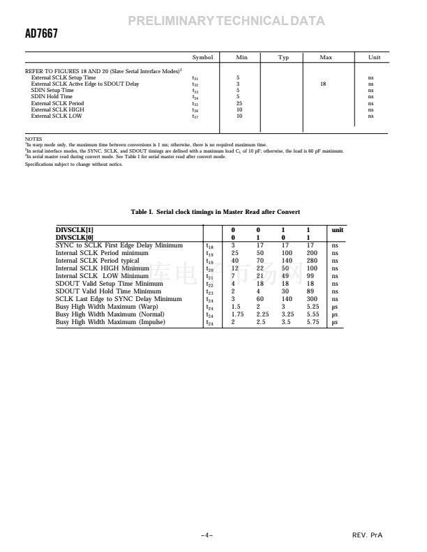
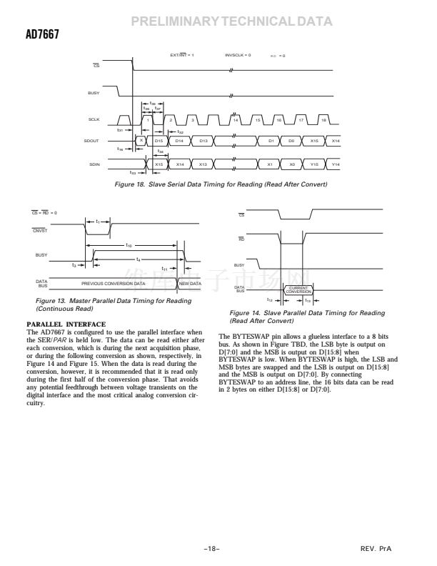
parallel interface. The serial interface is multiplexed on
the parallel data bus. The AD7667 digital interface also
accommodates both 3 V or 5 V logic by simply connecting
the OVDD supply pin of the AD7667 to the host system
interface digital supply. Finally, by using the OB/2C in-
put pin, both two鈥檚 complement or straight binary coding
can be used.
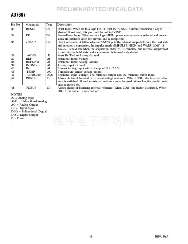
The two signals
CS
and
RD
control the interface.
CS
and
RD
have a similar effect because they are OR鈥檇 together inter-
nally. When at least one of these signals is high, the interface
outputs are in high impedance. Usually,
CS
allows the selec-
tion of each AD7667 in multicircuits applications and is held
low in a single AD7667 design.
RD
is generally used to
enable the conversion result on the data bus.
CS, RD
EXT/INT = 0
RDC/SDIN = 0
INVSCLK = INVSYNC = 0
t
3
CNVST
BUSY
t
28
t
30
t
29
SYNC
t
25
t
18
t
19
t
14
t
20
SCLK
t
21
1
2
3
14
15
t
24
16
t
26
t
15
t
27
SDOUT
X
D15
D14
D2
D1
D0
t
16
t
22
t
23
Figure 16. Master Serial Data Timing for Reading (Read After Convert)
EXT/INT = 0
CS, RD
RDC/SDIN = 1
INVSCLK = INVSYNC = 0
t
1
CNVST
t
3
BUSY
t
17
SYNC
t
25
t
14
t
19
t
20
t
21
2
3
14
15
16
t
24
SCLK
t
15
t
26
1
t
18
t
27
SDOUT
X
D15
D14
D2
D1
D0
t
16
t
22
t
23
Figure 17. Master Serial Data Timing for Reading (Read Previous Conversion During Convert)
REV. PrA
鈥?7鈥?/div>
prev
next


 1
1
 2
2
 3
3
 4
4
 5
5
 6
6
 7
7
 8
8
 9
9
 10
10
 11
11
 12
12
 13
13
 14
14
 15
15
 16
16
 17
17
 18
18
 19
19
 20
20
 21
21
 22
22
 23
23
