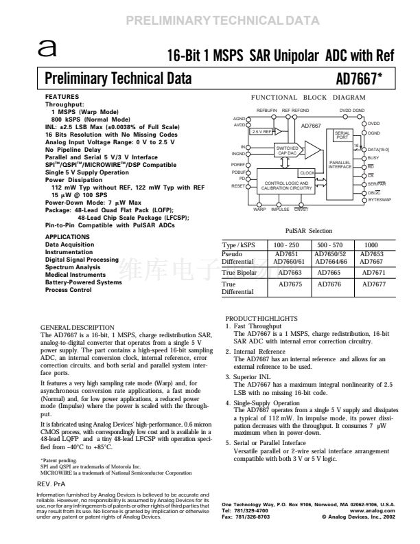
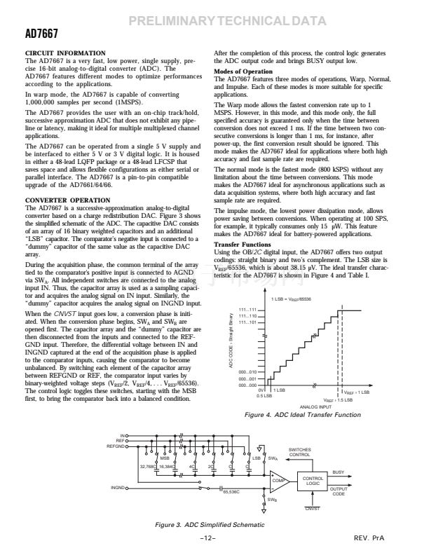
PRELIMINARY TECHNICAL DATA
AD7667
ABSOLUTE MAXIMUM RATINGS*
IN
2
, TEMP
2
,REF, REFBUFIN, INGND, REFGND to AGND
. . . . . . . . . . . . . . . . . . . . . . . AVDD + 0.3 V to AGND 鈥?0.3 V
Ground Voltage Differences
AGND, DGND, OGND . . . . . . . . . . . . . . . . . . . . . 卤0.3 V
Supply Voltages
AVDD, DVDD, OVDD . . . . . . . . . . . . . . . -0.3V to +7 V
AVDD to DVDD, AVDD to OVDD . . . . . . . . . . . . . 卤7 V
DVDD to OVDD . . . . . . . . . . . . . . . . . . . . -0.3V to +7 V
Digital Inputs . . . . . . . . . . . . . . . . 鈥?.3 V to DVDD + 3.0 V
Internal Power Dissipation
3
. . . . . . . . . . . . . . . . . . . 700 mW
Internal Power Dissipation
4
. . . . . . . . . . . . . . . . . . . . . 2.5 W
Junction Temperature . . . . . . . . . . . . . . . . . . . . . . . . . 150掳C
Storage Temperature Range . . . . . . . . . . . . 鈥?5掳C to +150掳C
Lead Temperature Range
(Soldering 10 sec) . . . . . . . . . . . . . . . . . . . . . . . . . . . 300掳C
NOTES
1
Stresses above those listed under Absolute Maximum Ratings may cause perma-
nent damage to the device. This is a stress rating only; functional operation of the
device at these or any other conditions above those listed in the operational
sections of this specification is not implied. Exposure to absolute maximum rating
conditions for extended periods may affect device reliability.
2
See Analog Input section.
3
Specification is for the device in free air:
48-Lead LQFP;
胃
JA
= 91掳C/W,
胃
JC
= 30掳C/W
4
Specification is for the device in free air:
48-Lead LFCSP;
胃
JA
= 26掳C/W
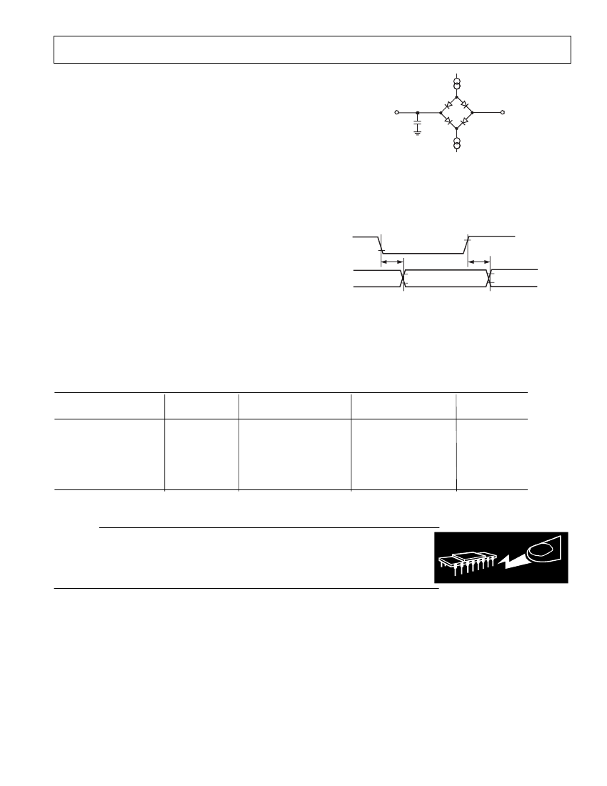
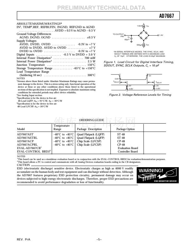
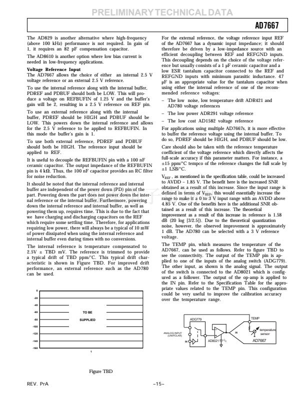
1.6mA
I
OL
TO OUTPUT
PIN
1.4V
C
L
60pF*
500 A
I
OH
*IN
SERIAL INTERFACE MODES, THE SYNC, SCLK, AND
SDOUT TIMINGS ARE DEFINED WITH A MAXIMUM LOAD
C
L
OF 10pF; OTHERWISE, THE LOAD IS 60pF MAXIMUM.
Figure 1. Load Circuit for Digital Interface Timing,
SDOUT, SYNC, SCLK Outputs, C
L
= 10 pF
2V
0.8V
t
DELAY
2V
0.8V
t
DELAY
2V
0.8V
Figure 2. Voltage Reference Levels for Timing
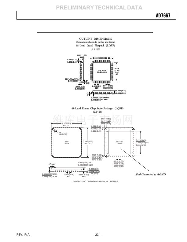
ORDERING GUIDE
Model
AD7667AST
AD7667ASTRL
AD7667ACP
AD7667ACPRL
EVAL-AD7667CB
1
EVAL-CONTROL BRD2
2
Temperature
Range
鈥?0掳C
鈥?0掳C
鈥?0掳C
鈥?0掳C
to
to
to
to
+85掳C
+85掳C
+85掳C
+85掳C
Package Description
Quad Flatpack (LQFP)
Quad Flatpack (LQFP)
Chip Scale (LFCSP)
Chip Scale (LFCSP)
Package Option
ST-48
ST-48
CP-48
CP-48
Evaluation Board
Controller Board
NOTES
1
This board can be used as a standalone evaluation board or in conjunction with the EVAL-CONTROL BRD2 for evaluation/demonstration purposes.
2
This board allows a PC to control and communicate with all Analog Devices evaluation boards ending in the CB designators.
CAUTION
ESD (electrostatic discharge) sensitive device. Electrostatic charges as high as 4000 V readily
accumulate on the human body and test equipment and can discharge without detection. Although
the AD7667 features proprietary ESD protection circuitry, permanent damage may occur on
devices subjected to high-energy electrostatic discharges. Therefore, proper ESD precautions are
recommended to avoid performance degradation or loss of functionality.
WARNING!
ESD SENSITIVE DEVICE
REV. PrA
鈥?鈥?/div>
prev
next


 1
1
 2
2
 3
3
 4
4
 5
5
 6
6
 7
7
 8
8
 9
9
 10
10
 11
11
 12
12
 13
13
 14
14
 15
15
 16
16
 17
17
 18
18
 19
19
 20
20
 21
21
 22
22
 23
23
