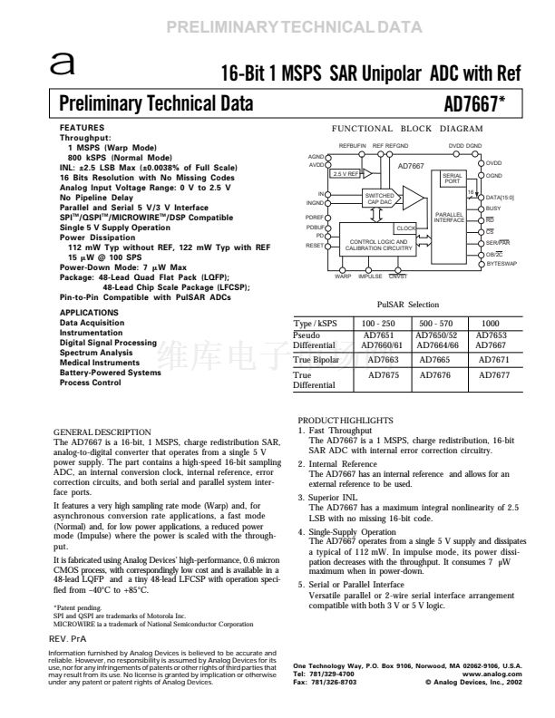
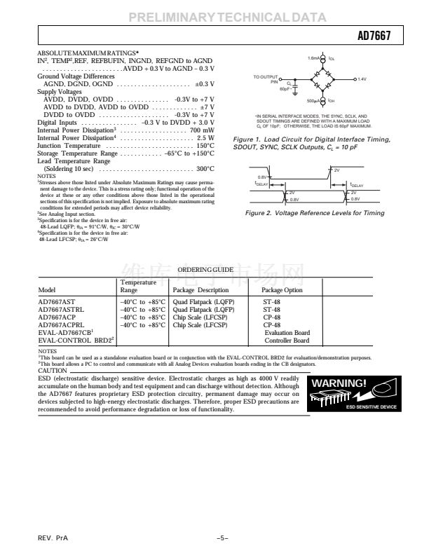
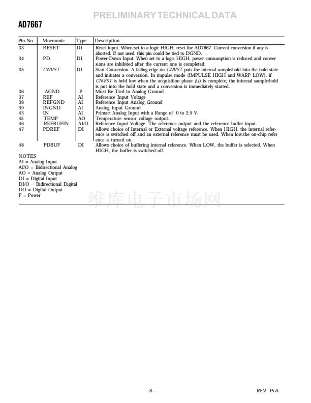
PRELIMINARY TECHNICAL DATA
AD7667
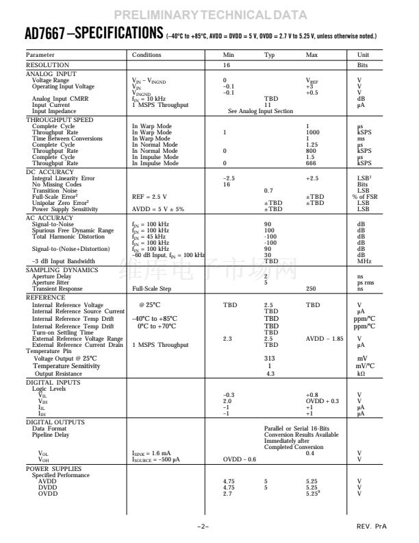
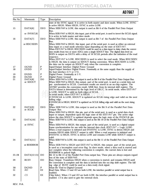
PIN CONFIGURATION
48-Lead LQFP
(ST-48)
PDBUF
PDREF
REFBUFIN
TEMP
NC
IN
NC
NC
NC
AGND
1
AVDD
2
NC
BYTESWAP
OB/2C
WARP
IMPULSE
SER/PAR
D0
D1
D2/SCLK0
D3/SCLK1
3
4
5
6
7
8
9
10
11
12
13 14 15 16 17 18 19 20 21 22 23 24
48 47 46 45 44 43 42 41 40 39 38 37
PIN 1
IDENTIFIER
36
AGND
35
CNVST
34
PD
33
RESET
32
CS
31
RD
30
DGND
29
BUSY
28
D15
27
D14
26
D13
25
D12
AD7667
TOP VIEW
(Not to Scale)
D4/EXT/INT
D5/INVSYNC
D6/INVSCLK
D7/RDC/SDIN
OGND
OVDD
DVDD
DGND
D8/SDOUT
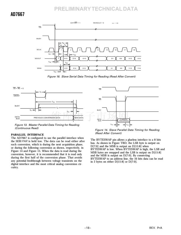
PIN FUNCTION DESCRIPTIONS
Pin No.
1
2
3, 40鈥?2,
44
4
Mnemonic
AGND
AVDD
NC
BYTESWAP
Type
P
P
Description
Analog Power Ground Pin
Input Analog Power Pins. Nominally 5 V.
No Connect
Parallel Mode Selection (8/16 bit). When LOW, the LSB is output on D[7:0] and the
MSB is output on D[15:8]. When HIGH, the LSB is output on D[15:8] and the MSB
is output on D[7:0].
Straight Binary/Binary Two鈥檚 Complement. When OB/2C is HIGH, the digital output is
straight binary; when LOW, the MSB is inverted resulting in a two鈥檚 complement output
from its internal shift register.
Mode Selection. When HIGH and IMPULSE LOW, this input selects the fastest mode,
the maximum throughput is achievable, and a minimum conversion rate must be applied
in order to guarantee full specified accuracy. When LOW, full accuracy is maintained
independent of the minimum conversion rate.
Mode Selection. When HIGH and WARP LOW, this input selects a reduced power mode.
In this mode, the power dissipation is approximately proportional to the sampling rate.
Serial/Parallel Selection Input. When LOW, the parallel port is selected; when HIGH, the
serial interface mode is selected and some bits of the DATA bus are used as a serial port.
Bit 0 and Bit 1 of the Parallel Port Data Output Bus. When SER/PAR is HIGH, these
outputs are in high impedance.
When SER/PAR is LOW, these outputs are used as Bit 2 and Bit 3 of the Parallel Port
Data Output Bus. When SER/PAR is HIGH, EXT/INT is LOW, and RDC/SDIN is
LOW, which is serial master read after convert, these inputs, part of the serial port, are
used to slow down if desired the internal serial clock which clocks the data output. In
other serial moes, these pins are not used
When SER/PAR is LOW, this output is used as Bit 4 of the Parallel Port Data Output
Bus.
When SER/PAR is HIGH, this input, part of the serial port, is used as a digital select input
for choosing the internal or an external data clock. With EXT/INT tied LOW, the internal
clock is selected on SCLK output. With EXT/INT set to a logic HIGH, output data is syn
chronized to an external clock signal connected to the SCLK input.
When SER/PAR is LOW, this output is used as Bit 5 of the Parallel Port Data Output
Bus.
When SER/PAR is HIGH, this input, part of the serial port, is used to select the active
鈥?鈥?/div>
REV. PrA
DI
5
OB/2C
DI
6
WARP
DI
7
8
9,10
11,12
IMPULSE
SER/PAR
DATA[0:1]
DATA[2:3]or
DIVSCLK[0:1]
DI
DI
DI
DI/O
13
DATA[4]
or EXT/INT
DI/O
14
DATA[5]
or INVSYNC
DI/O
D9/SCLK
D10/SYNC
D11/RDERROR
NC = NO CONNECT
INGND
REFGND
REF


 1
1
 2
2
 3
3
 4
4
 5
5
 6
6
 7
7
 8
8
 9
9
 10
10
 11
11
 12
12
 13
13
 14
14
 15
15
 16
16
 17
17
 18
18
 19
19
 20
20
 21
21
 22
22
 23
23
