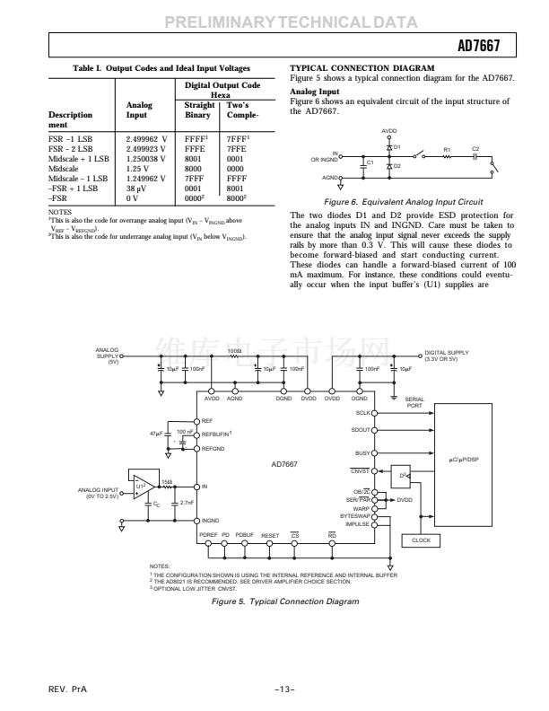
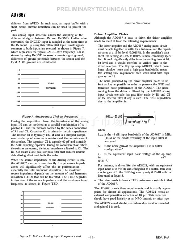
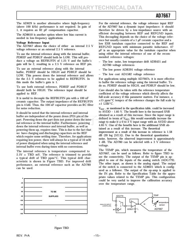
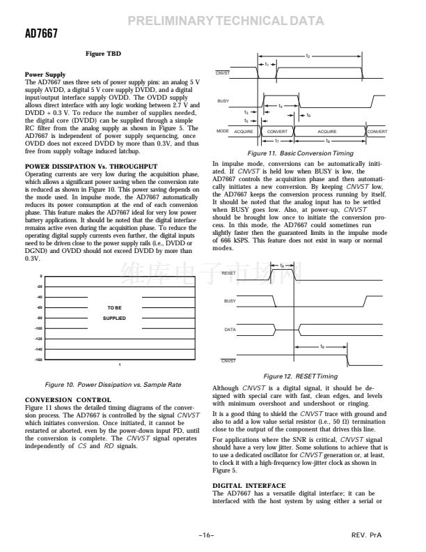
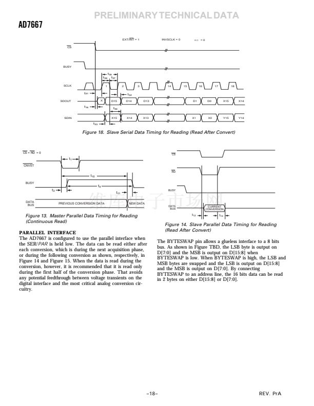
PRELIMINARY TECHNICAL DATA
AD7667
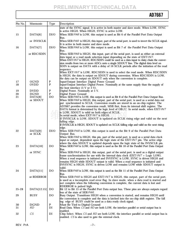
Pin No.
Mnemonic
Type
Description
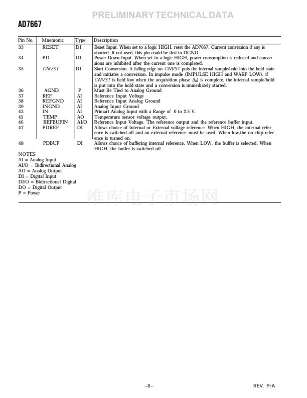
state of the SYNC signal. It is active in both master and slave mode. When LOW, SYNC
is active HIGH. When HIGH, SYNC is active LOW.
When SER/PAR is LOW, this output is used as Bit 6 of the Parallel Port Data Output
Bus.
When SER/PAR is HIGH, this input, part of the serial port, is used to invert the SCLK signal.
It is active in both master and slave mode.
When SER/PAR is LOW, this output is used as Bit 7 of the Parallel Port Data Output
Bus.
When SER/PAR is HIGH, this input, part of the serial port, is used as either an external
data input or a read mode selection input depending on the state of EXT/INT.
When EXT/INT is HIGH, RDC/SDIN could be used as a data input to daisy chain the conver-
sion results from two or more ADCs onto a single SDOUT line. The digital data level on
SDIN is output on DATA with a delay of 16 SCLK periods after the initiation of the read
sequence.
When EXT/INT is LOW, RDC/SDIN is used to select the read mode. When RDC/SDIN
is HIGH, the data is output on SDOUT during conversion. When RDC/SDIN is LOW,
the data can be output on SDOUT only when the conversion is complete.
Input/Output Interface Digital Power Ground
Input/Output Interface Digital Power. Nominally at the same supply than the supply of
the host interface (5 V or 3 V).
Digital Power. Nominally at 5 V.
Digital Power Ground
When SER/PAR is LOW, this output is used as Bit 8 of the Parallel Port Data Output Bus.
When SER/PAR is HIGH, this output, part of the serial port, is used as a serial data out
put synchronized to SCLK. Conversion results are stored in an on-chip register. The
AD7667 provides the conversion result, MSB first, from its internal shift register. The
DATA format is determined by the logic level of OB/2C. In serial mode, when EXT/INT
is LOW, SDOUT is valid on both edges of SCLK.
In serial mode, when EXT/INT is HIGH:
If INVSCLK is LOW, SDOUT is updated on SCLK rising edge and valid on the next
falling edge.
If INVSCLK is HIGH, SDOUT is updated on SCLK falling edge and valid on the next rising
edge.
When SER/PAR is LOW, this output is used as the Bit 9 of the Parallel Port Data
Output Bus.
When SER/PAR is HIGH, this pin, part of the serial port, is used as a serial data clock
input or output, dependent upon the logic state of the EXT/INT pin. The active edge
where the data SDOUT is updated depends upon the logic state of the INVSCLK pin.
When SER/PAR is LOW, this output is used as the Bit 10 of the Parallel Port Data Output
Bus.
When SER/PAR is HIGH, this output, part of the serial port, is used as a digital output
frame synchronization for use with the internal data clock (EXT/INT = Logic LOW).
When a read sequence is initiated and INVSYNC is LOW, SYNC is driven HIGH and
remains HIGH while SDOUT output is valid. When a read sequence is initiated and
INVSYNC is HIGH, SYNC is driven LOW and remains LOW while SDOUT output is
valid.
When SER/PAR is LOW, this output is used as the Bit 11 of the Parallel Port Data Output
Bus.
When SER/PAR is HIGH and EXT/INT is HIGH, this output, part of the serial port,
is used as a incomplete read error flag. In slave mode, when a data read is started and
not complete when the following conversion is complete, the current data is lost and
RDERROR is pulsed high.
Bit 12 to Bit 15 of the Parallel Port Data output bus. These pins are always outputs regard
less of the state of SER/PAR.
Busy Output. Transitions HIGH when a conversion is started, and remains HIGH until
the conversion is complete and the data is latched into the on-chip shift register. The fall
ing edge of BUSY could be used as a data ready clock signal.
Must Be Tied to Digital Ground
Read Data. When
CS
and
RD
are both LOW, the interface parallel or serial output bus is
enabled.
Chip Select. When
CS
and
RD
are both LOW, the interface parallel or serial output bus is
enabled.
CS
is also used to gate the external clock.
鈥?鈥?/div>
15
DATA[6]
or INVSCLK
DI/O
16
DATA[7]
or RDC/SDIN
DI/O
17
18
19
20
21
OGND
OVDD
DVDD
DGND
DATA[8]
or SDOUT
P
P
P
P
DO
22
DATA[9]
or SCLK
DI/O
23
DATA[10]
or SYNC
DO
24
DATA[11]
or RDERROR
DO
25鈥?8
29
30
31
32
DATA[12:15] DO
BUSY
DGND
RD
CS
DO
P
DI
DI
REV. PrA


 1
1
 2
2
 3
3
 4
4
 5
5
 6
6
 7
7
 8
8
 9
9
 10
10
 11
11
 12
12
 13
13
 14
14
 15
15
 16
16
 17
17
 18
18
 19
19
 20
20
 21
21
 22
22
 23
23
