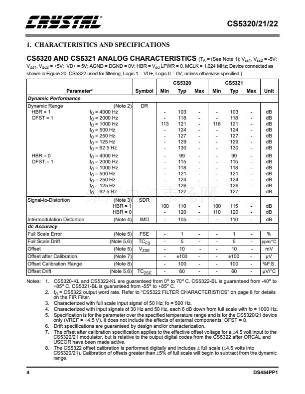
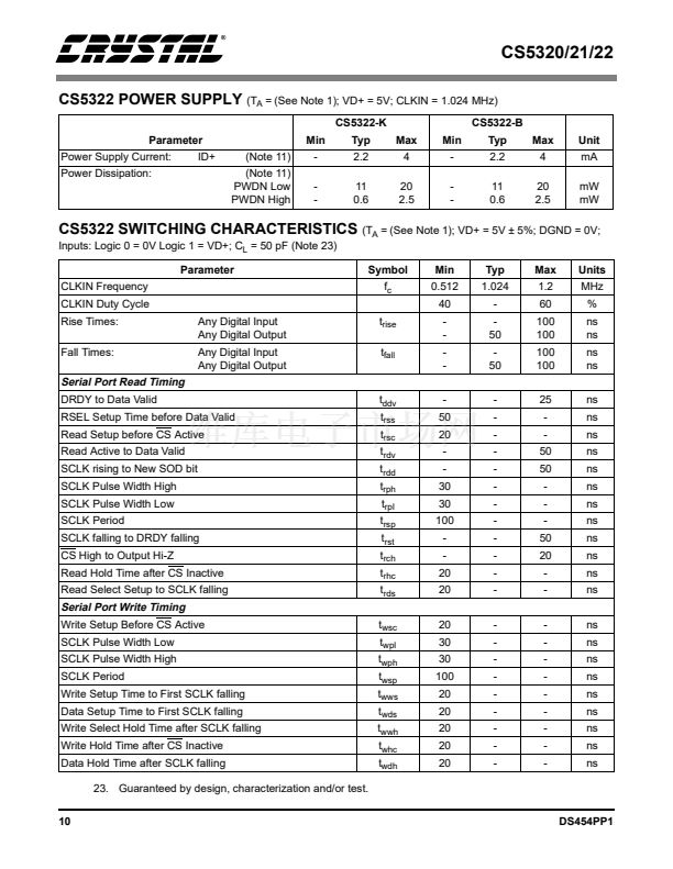
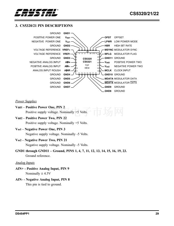
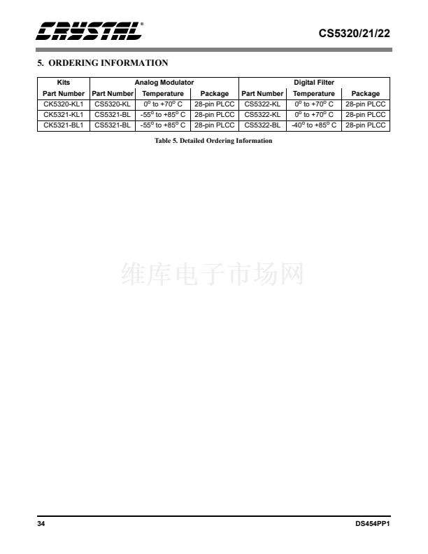
voltage reference inputs. The signal input uses three
pins; AINR, AIN+, and AIN-. The AIN- pin acts as
the return pin for the AINR and AIN+ pins. The
put for the AIN+ pin. The input impedance for the
the internal sampling capacitor (about 40 pF). Us-
the impedance seen on the AINR pin.
over temperature and from device to device. There-
should be driven from a low source impedance.
鈩?/div>
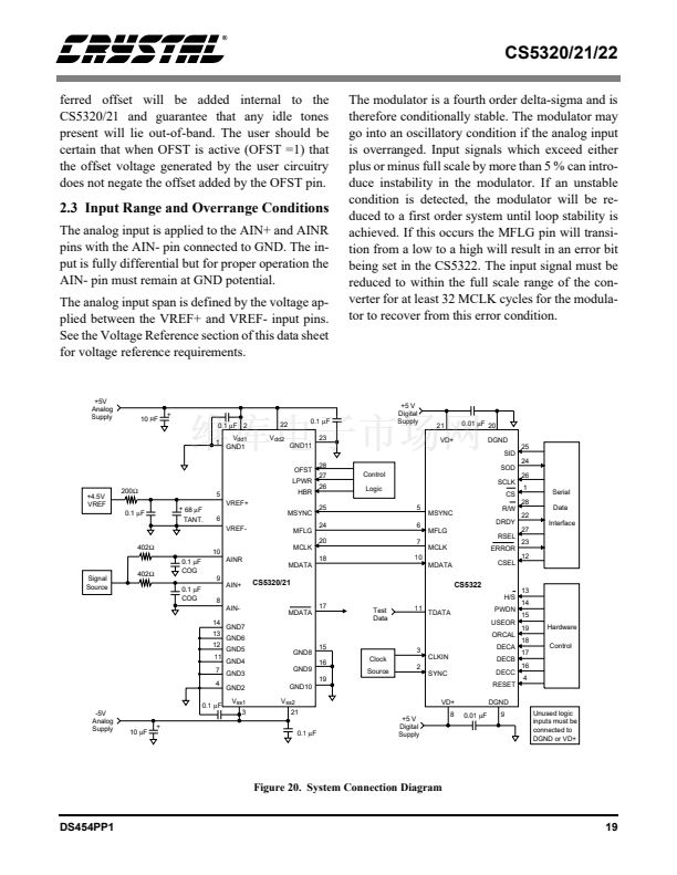
source resistor of Figure 20 and Figure 21
Option A with MCLK = 1.024 MHz, HBR = 1, and
temperature = 25掳C.
When the CS5320/21 modulator is operated with a
4.5 V reference it will accept a 9 V p-p input signal,
but modulator loop stability can be adversely af-
fected by high frequency out-of-band signals.
Therefore, input signals must be band-limited by an
input filter. The -3 dB corner of the input filter must
be equal to the modulator sampling clock divided
by 64. The modulator sampling clock is MCLK/4
when HBR = 1 or MCLK/8 when HBR = 0. With
MCLK = 1.024 MHz, HBR = 1, the modulator
sampling clock is 256 kHz which requires an input
filter with a -3 dB corner of 4 kHz. The bandlimit-
ing may be accomplished in an amplifier stage
ahead of the CS5320/21 modulator or with the RC
input filter at the AIN+ and AINR input pins. The
RC filter at the AIN+ and AINR pins is recom-
mended to reduce the "charge kick" that the driving
amplifier sees as the switched capacitor sampling is
performed.
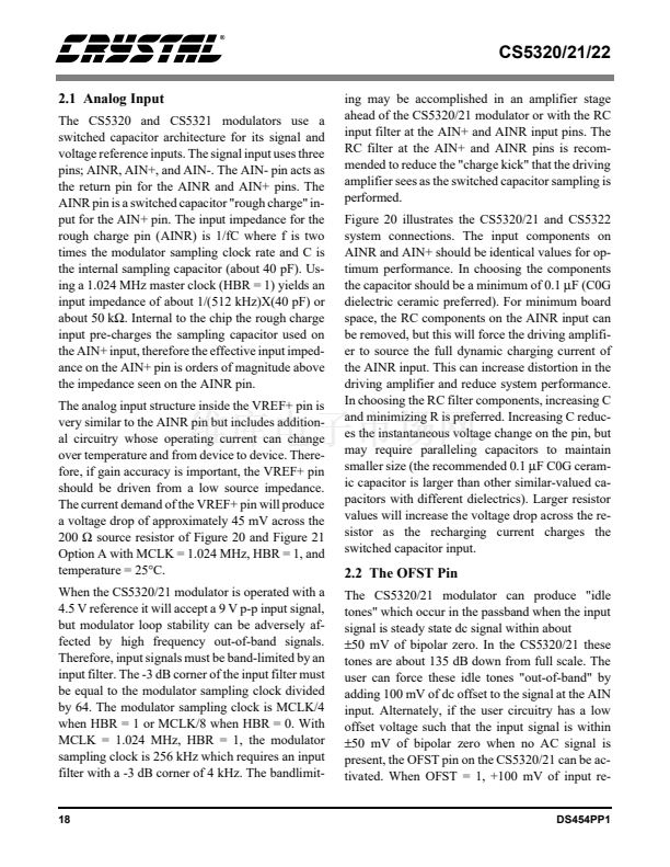
Figure 20 illustrates the CS5320/21 and CS5322
system connections. The input components on
AINR and AIN+ should be identical values for op-
timum performance. In choosing the components
the capacitor should be a minimum of 0.1
碌F
(C0G
dielectric ceramic preferred). For minimum board
space, the RC components on the AINR input can
be removed, but this will force the driving amplifi-
er to source the full dynamic charging current of
the AINR input. This can increase distortion in the
driving amplifier and reduce system performance.
In choosing the RC filter components, increasing C
and minimizing R is preferred. Increasing C reduc-
es the instantaneous voltage change on the pin, but
may require paralleling capacitors to maintain
smaller size (the recommended 0.1
碌F
C0G ceram-
ic capacitor is larger than other similar-valued ca-
pacitors with different dielectrics). Larger resistor
values will increase the voltage drop across the re-
sistor as the recharging current charges the
switched capacitor input.
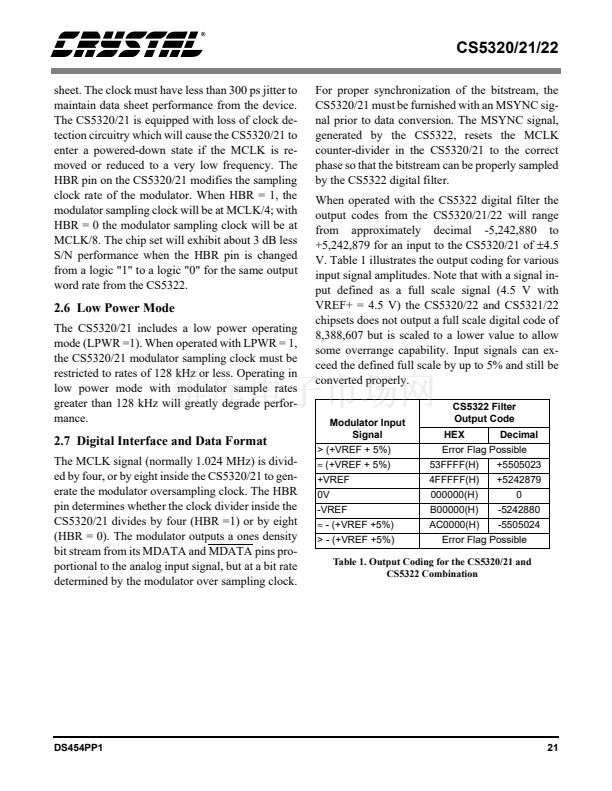
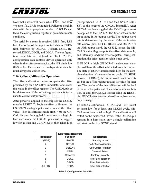
2.2 The OFST Pin
The CS5320/21 modulator can produce "idle
tones" which occur in the passband when the input
signal is steady state dc signal within about
卤50
mV of bipolar zero. In the CS5320/21 these
tones are about 135 dB down from full scale. The
user can force these idle tones "out-of-band" by
adding 100 mV of dc offset to the signal at the AIN
input. Alternately, if the user circuitry has a low
offset voltage such that the input signal is within
卤50
mV of bipolar zero when no AC signal is
present, the OFST pin on the CS5320/21 can be ac-
tivated. When OFST = 1, +100 mV of input re-
DS454PP1
18


 1
1
 2
2
 3
3
 4
4
 5
5
 6
6
 7
7
 8
8
 9
9
 10
10
 11
11
 12
12
 13
13
 14
14
 15
15
 16
16
 17
17
 18
18
 19
19
 20
20
 21
21
 22
22
 23
23
 24
24
 25
25
 26
26
 27
27
 28
28
 29
29
 30
30
 31
31
 32
32
 33
33
 34
34
 35
35
 36
36
 37
37
 38
38
