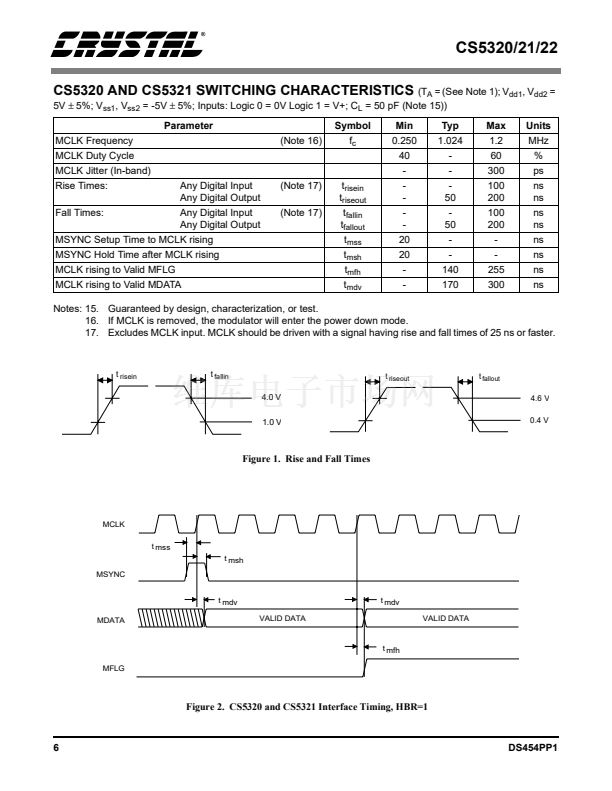
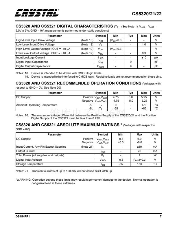
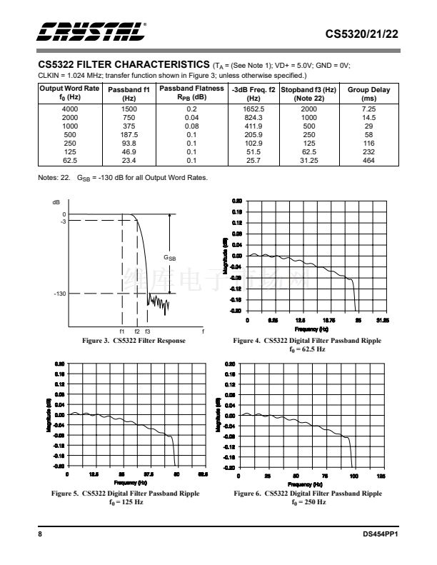
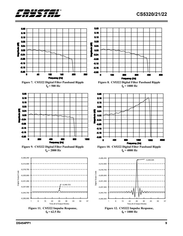
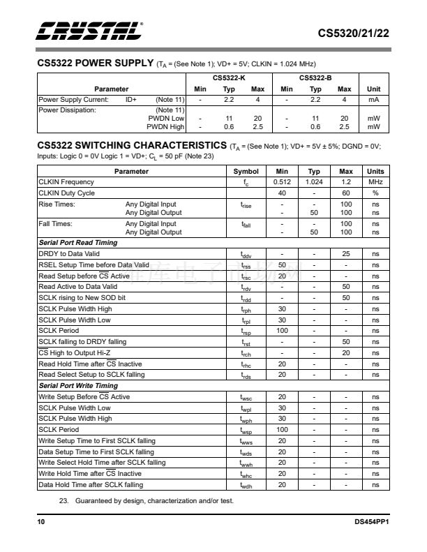
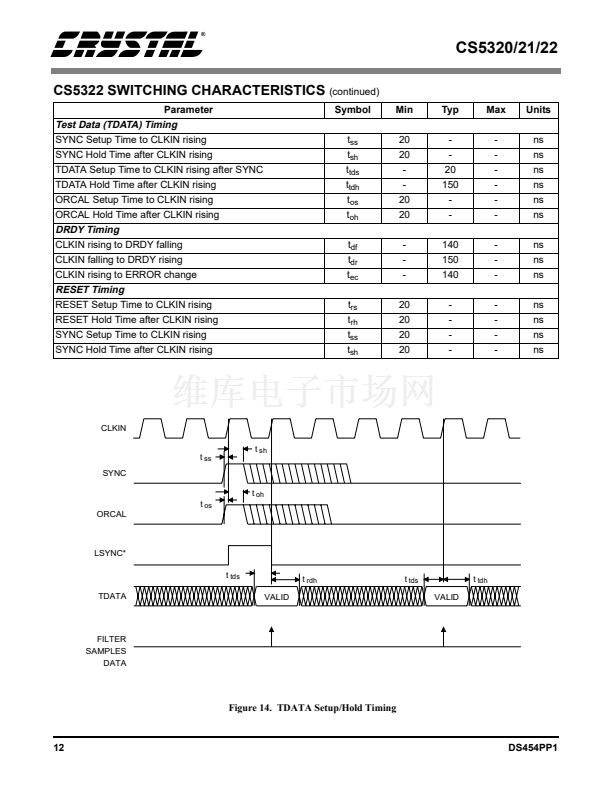
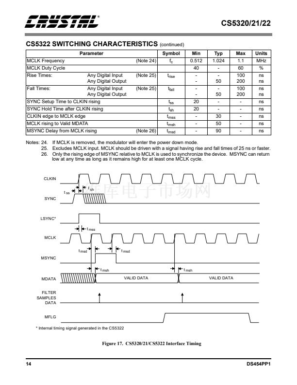
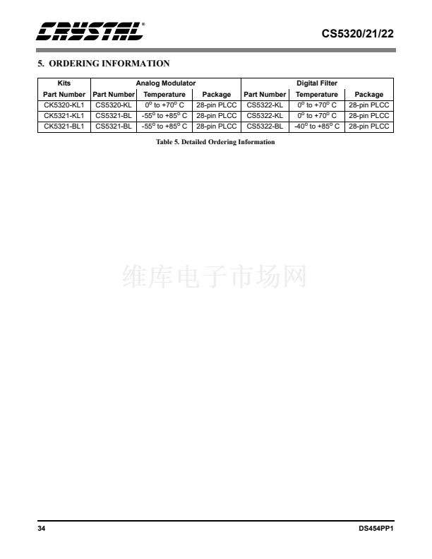
CS5320/21/22
Note that a write will occur when CS = 0 and R/W
= 0 even if SCLK is not toggled. Failure to clock in
data with the appropriate number of SCLKs can
leave the configuration register in an indeterminate
condition.
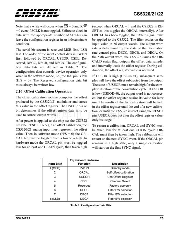
The serial bit stream is received MSB first, LSB
last. The order of the input control data is PWDN
first, followed by ORCAL, USEOR, CSEL, Re-
served, DECC, DECB, and DECA. The configura-
tion data bits are defined in Table 2. The
configuration data controls device operation only
when in the software mode, i.e., the H/S pin is low
(H/S = 0). The Reserved configuration data bit
must always be written low.
(except when ORCAL = 1 and the CS5322 is RE-
SET as this toggles the ORCAL internally). After
ORCAL has been toggled, the SYNC signal must
be applied to the CS5322. The filter settles on the
input value in 56 output words. The output word
rate is determined by the state of the decimation
rate control pins, DECC, DECB, and DECA. On
the 57th output word, the CS5322 issues the OR-
CALD status flag, outputs the offset data sample,
and internally loads the offset register. During cal-
ibration, the offset register value is not used.
If USEOR is high (USEOR=1), subsequent sam-
ples will have the offset subtracted from the output.
The state of USEOR must remain high for the com-
plete duration of the convolution cycle. If USEOR
is low (USEOR=0), the output word is not correct-
ed, but the offset register retains its value for later
use. The results of the last calibration will be held
in the offset register until the end of a new calibra-
tion, or until the CS5322 is reset using the RESET
pin. USEOR does not alter the offset register value,
only its usage.
To restart a calibration, ORCAL and SYNC must
be taken low for at least one CLKIN cycle. OR-
CAL must then be taken high. The calibration will
restart on the next SYNC event. If the ORCAL pin
remains in a high state, only a single calibration
will start on the first SYNC signal.
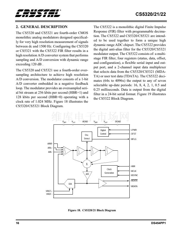
2.16 Offset Calibration Operation
The offset calibration routine computes the offset
produced by the CS5320/21 modulator and stores
this value in the offset register. The USEOR pin or
bit determines if the offset register data is to be
used to correct output words.
After power is applied to the chip set the CS5322
must be RESET. To begin an offset calibration, the
CS5320/21 analog input must represent the offset
value. Then in software mode (H/S = 0) the OR-
CAL bit must be toggled from a low to a high. In
hardware mode the ORCAL pin must be toggled
low for at least one CLKIN cycle, then taken high
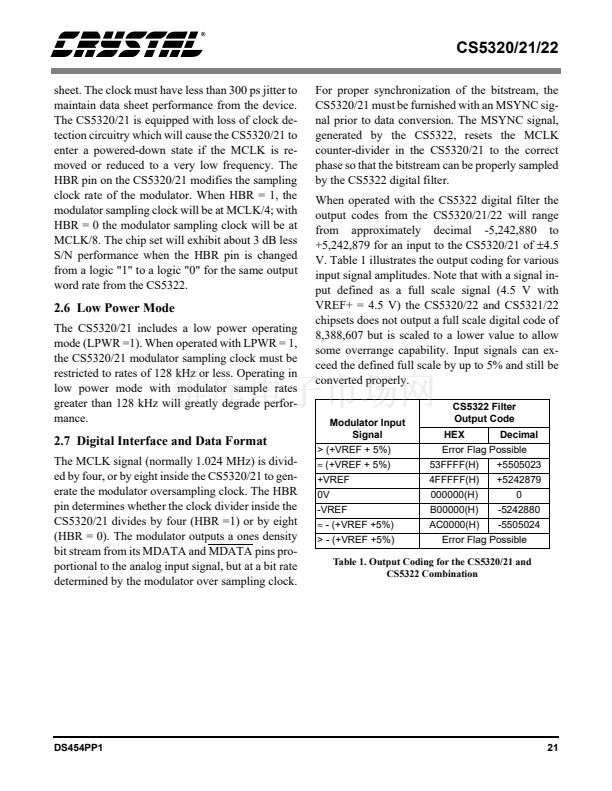
Input Bit #
1 (MSB)
2
3
4
5
6
7
8 (LSB)
Equivalent Hardware
Function
PWDN
ORCAL
USEOR
CSEL
Reserved
DECC
DECB
DECA
Description
Standby mode
Self-offset calibration
Use Offset Register
Channel Select
Factory use only
Filter BW selection
Filter BW selection
Filter BW selection
Table 2. Configuration Data Bits
DS454PP1
25


 1
1
 2
2
 3
3
 4
4
 5
5
 6
6
 7
7
 8
8
 9
9
 10
10
 11
11
 12
12
 13
13
 14
14
 15
15
 16
16
 17
17
 18
18
 19
19
 20
20
 21
21
 22
22
 23
23
 24
24
 25
25
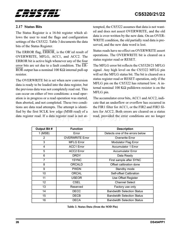 26
26
 27
27
 28
28
 29
29
 30
30
 31
31
 32
32
 33
33
 34
34
 35
35
 36
36
 37
37
 38
38
