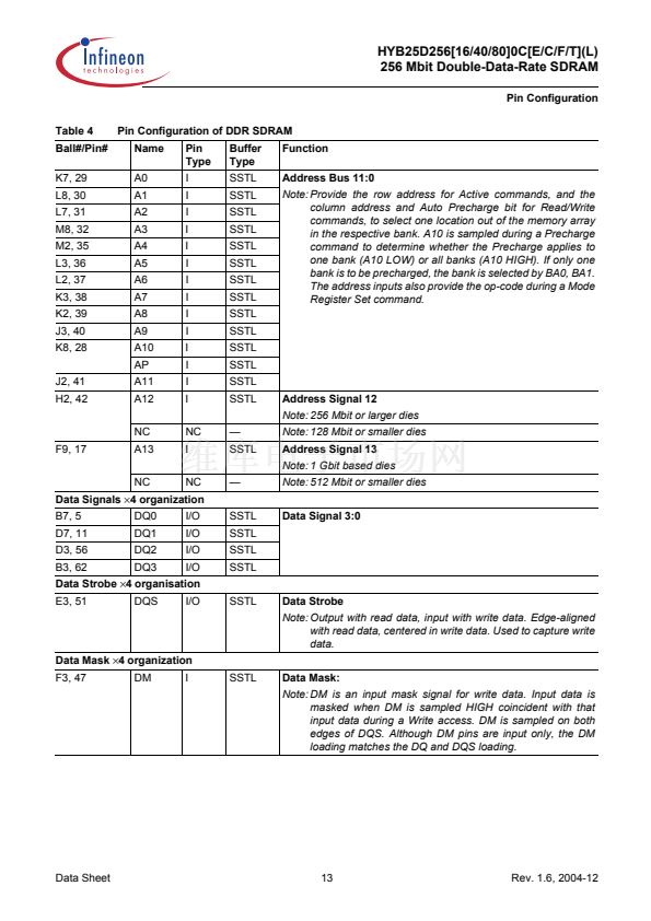
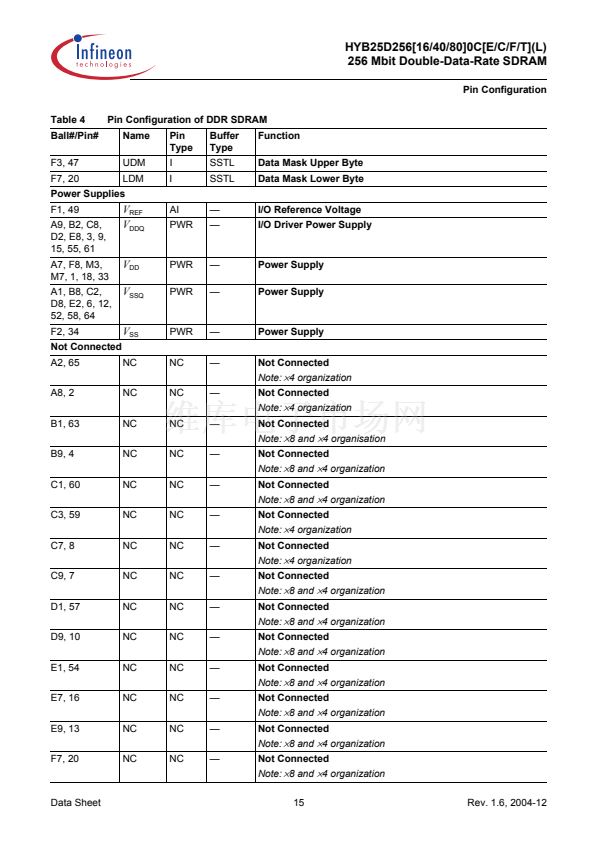
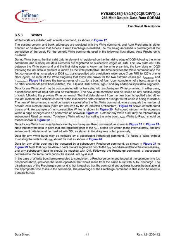
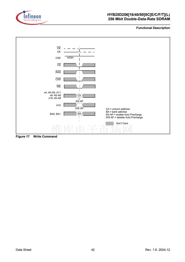
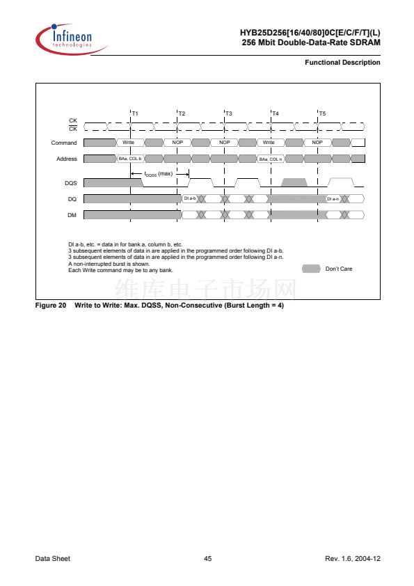
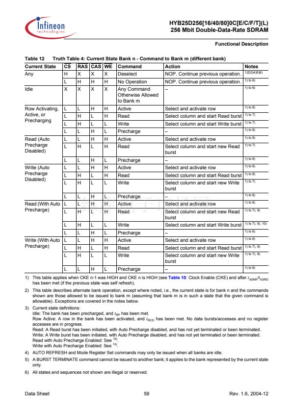
HYB25D256[16/40/80]0C[E/C/F/T](L)
256 Mbit Double-Data-Rate SDRAM
Overview
1.2
Description
The 256 Mbit Double-Data-Rate SDRAM is a high-speed CMOS, dynamic random-access memory containing
268,435,456 bits. It is internally configured as a quad-bank DRAM.
The 256 Mbit Double-Data-Rate SDRAM uses a double-data-rate architecture to achieve high-speed operation.
The double data rate architecture is essentially a
2n
prefetch architecture with an interface designed to transfer
two data words per clock cycle at the I/O pins. A single read or write access for the
256 Mbit Double-Data-Rate SDRAM effectively consists of a single
2n-bit
wide, one clock cycle data transfer at
the internal DRAM core and two corresponding n-bit wide, one-half-clock-cycle data transfers at the I/O pins.
A bidirectional data strobe (DQS) is transmitted externally, along with data, for use in data capture at the receiver.
DQS is a strobe transmitted by the DDR SDRAM during Reads and by the memory controller during Writes. DQS
is edge-aligned with data for Reads and center-aligned with data for Writes.
The 256 Mbit Double-Data-Rate SDRAM operates from a differential clock (CK and CK; the crossing of CK going
HIGH and CK going LOW is referred to as the positive edge of CK). Commands (address and control signals) are
registered at every positive edge of CK. Input data is registered on both edges of DQS, and output data is
referenced to both edges of DQS, as well as to both edges of CK.Read and write accesses to the DDR SDRAM
are burst oriented; accesses start at a selected location and continue for a programmed number of locations in a
programmed sequence. Accesses begin with the registration of an Active command, which is then followed by a
Read or Write command. The address bits registered coincident with the Active command are used to select the
bank and row to be accessed. The address bits registered coincident with the Read or Write command are used
to select the bank and the starting column location for the burst access.
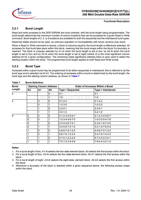
The DDR SDRAM provides for programmable Read or Write burst lengths of 2, 4 or 8 locations. An Auto
Precharge function may be enabled to provide a self-timed row precharge that is initiated at the end of the burst
access. As with standard SDRAMs, the pipelined, multibank architecture of DDR SDRAMs allows for concurrent
operation, thereby providing high effective bandwidth by hiding row precharge and activation time.
An auto refresh mode is provided along with a power-saving power-down mode. All inputs are compatible with the
JEDEC Standard for SSTL_2. All outputs are SSTL_2, Class II compatible.
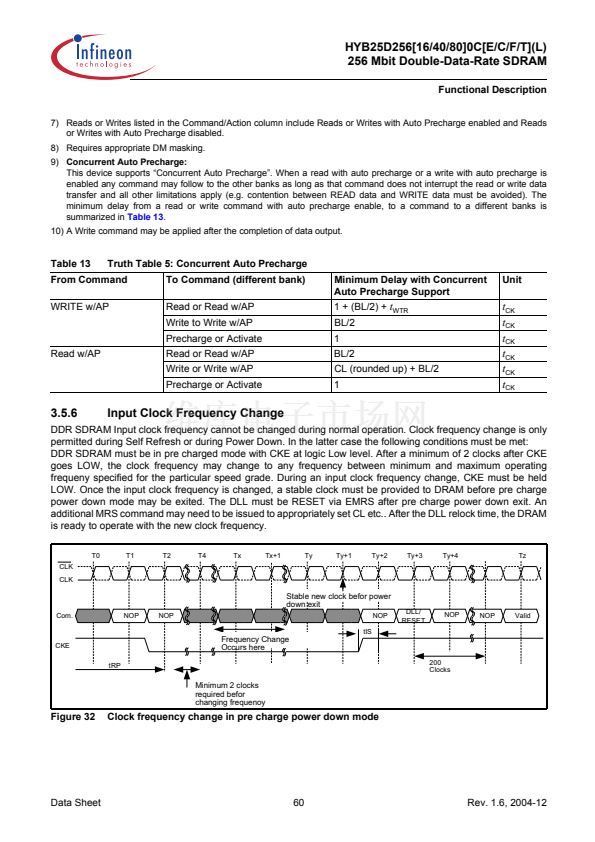
Note: The functionality described and the timing specifications included in this data sheet are for the DLL Enabled
mode of operation.
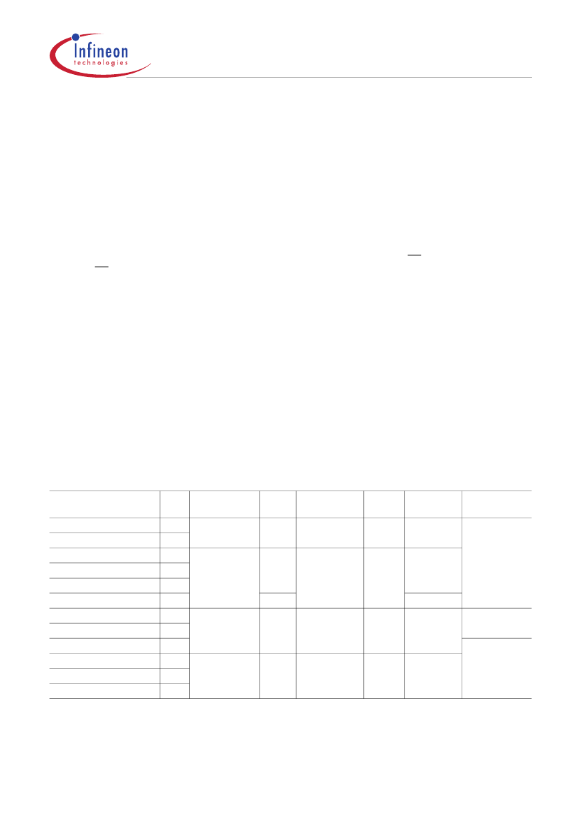
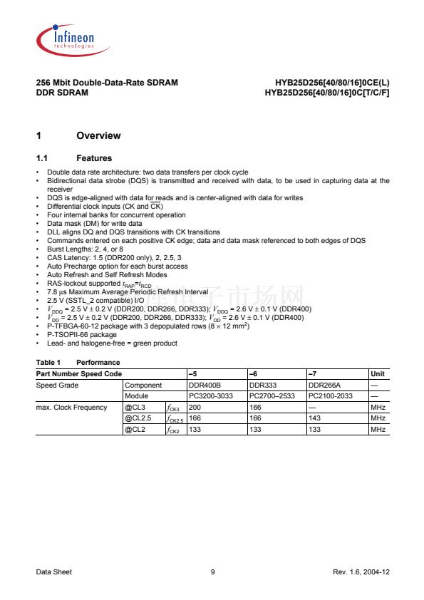
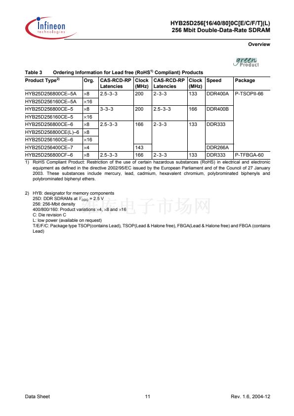
Table 2
Ordering Information for Lead Containing Products
Org. CAS-RCD-RP Clock
Latencies
(MHz)
脳8
脳16
脳8
脳16
脳4
脳4
脳8
脳16
脳4
脳8
脳16
2.5-3-3
166
2-3-3
133
DDR333
3-3-3
143
200
2.5-3-3
166
DDR266A
DDR400B
P-TFBGA-60
2.5-3-3
166
2-3-3
133
DDR333
3-3-3
200
CAS-RCD-RP Clock
Latencies
(MHz)
2.5-3-3
166
Speed
DDR400B
Package
P-TSOPII-66
Product Type
2)
HYB25D256800CT鈥?
HYB25D256160CT鈥?
HYB25D256800CT鈥?
HYB25D256160CT鈥?
HYB25D256400CT鈥?
HYB25D256400CC鈥?
HYB25D256800CC鈥?
HYB25D256160CC鈥?
HYB25D256400CC鈥?
HYB25D256800CC鈥?
HYB25D256160CC鈥?
HYB25D256800CT(L)鈥?
脳8
Data Sheet
10
Rev. 1.6, 2004-12


 1
1
 2
2
 3
3
 4
4
 5
5
 6
6
 7
7
 8
8
 9
9
 10
10
 11
11
 12
12
 13
13
 14
14
 15
15
 16
16
 17
17
 18
18
 19
19
 20
20
 21
21
 22
22
 23
23
 24
24
 25
25
 26
26
 27
27
 28
28
 29
29
 30
30
 31
31
 32
32
 33
33
 34
34
 35
35
 36
36
 37
37
 38
38
 39
39
 40
40
 41
41
 42
42
 43
43
 44
44
 45
45
 46
46
 47
47
 48
48
 49
49
 50
50
 51
51
 52
52
 53
53
 54
54
 55
55
 56
56
 57
57
 58
58
 59
59
 60
60
 61
61
 62
62
 63
63
 64
64
 65
65
 66
66
 67
67
 68
68
 69
69
 70
70
 71
71
 72
72
 73
73
 74
74
 75
75
 76
76
 77
77
 78
78
 79
79
 80
80
 81
81
 82
82
 83
83
 84
84
 85
85
 86
86
 87
87
 88
88
 89
89
 90
90
 91
91
 92
92
 93
93
 94
94
