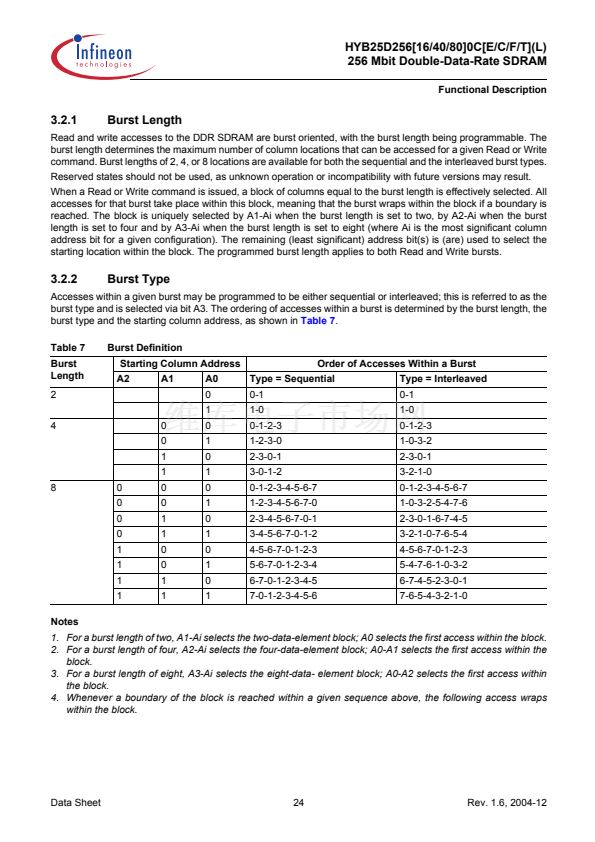
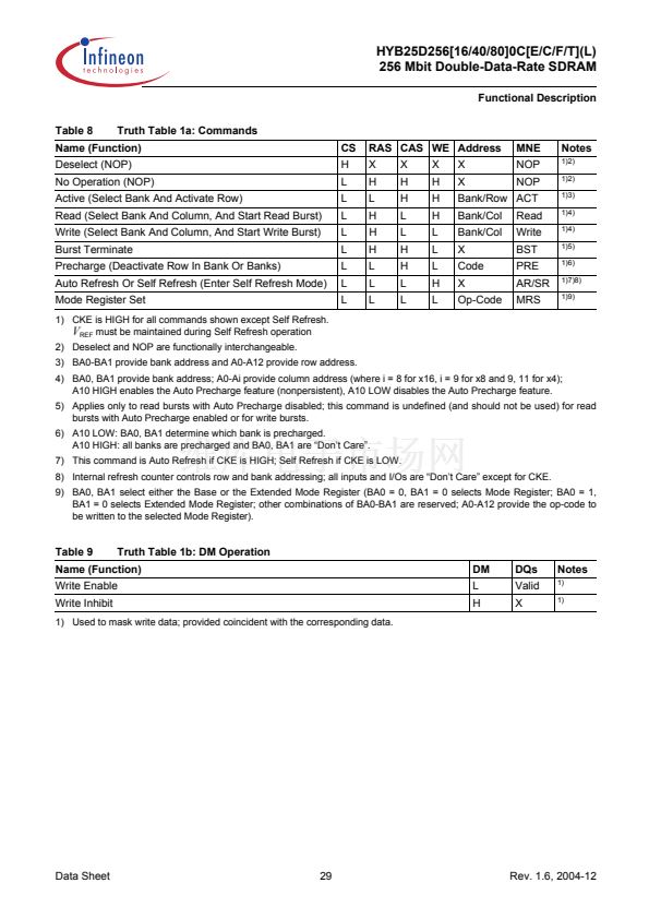
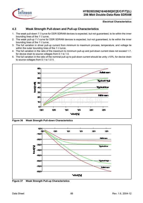
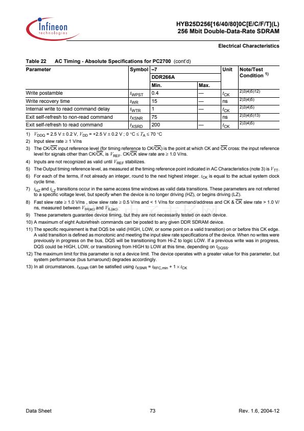
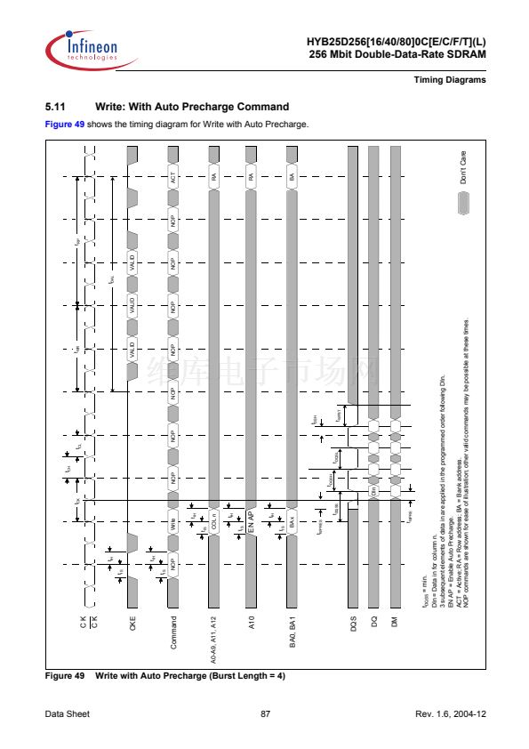
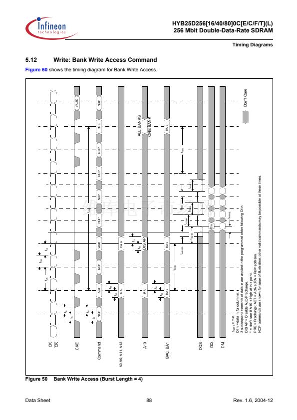
5.13
t
CH
t
CK
t
CL
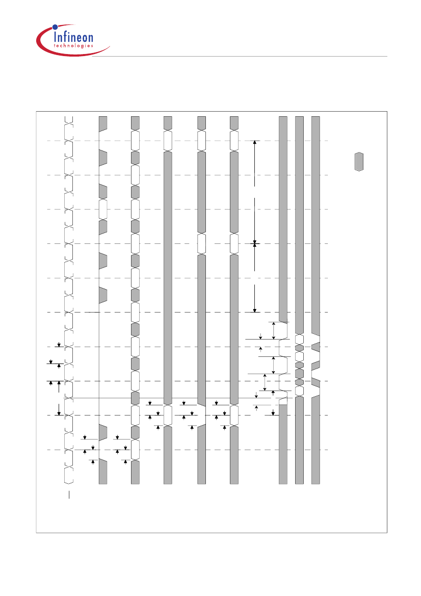
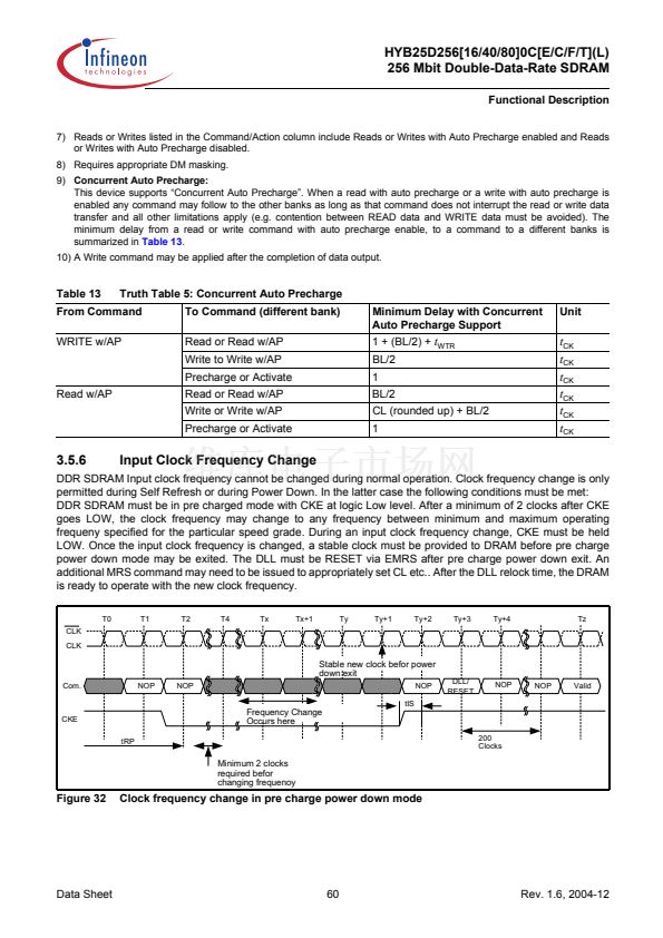
Figure 51
Data Sheet
VALID
NOP
NOP
NOP
NOP
PRE
NOP
NOP
ACT
CK
CK
t
IH
t
IS
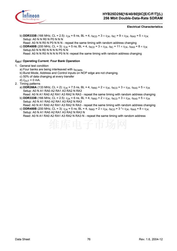
CKE
t
IH
t
IS
Command
t
IH
Write: DM Operation
NOP
Write
t
IS
COL n
RA
A0-A9, A11, A12
t
IH
t
IS
ALL BANKS
RA
Figure 51
shows the timing diagram for DM Operation.
Write DM Operation (Burst Length = 4)
ONE BANK
t
IH
A10
DIS AP
89
BA x
BA x*
t
WR
t
DQSH
t
DQSS
t
DQSL
t
WPST
t
DSH
DIn
t
IS
BA
BA0, BA1
t
WPRES
t
RP
DQS
DQ
DM
HYB25D256[16/40/80]0C[E/C/F/T](L)
256 Mbit Double-Data-Rate SDRAM
Timing Diagrams
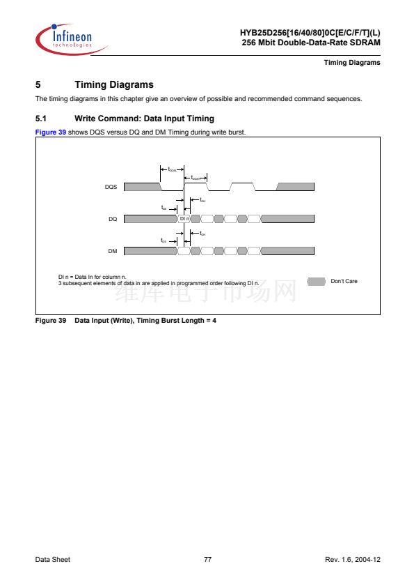
DI n = data in for column n.
3 subsequent elements of data in are applied in the programmed order following DI n (the second element of the 4 is masked).
DIS AP = Disable Auto Precharge.
*
= Don't care if A10 is High at this point.
PRE = Precharge; ACT = Active; RA = Row address; BA = Bank address.
NOP commands are shown for ease of illustration; other valid commands may be possible at these times.
t
DQSS
= min.
Rev. 1.6, 2004-12
Don鈥檛 Care


 1
1
 2
2
 3
3
 4
4
 5
5
 6
6
 7
7
 8
8
 9
9
 10
10
 11
11
 12
12
 13
13
 14
14
 15
15
 16
16
 17
17
 18
18
 19
19
 20
20
 21
21
 22
22
 23
23
 24
24
 25
25
 26
26
 27
27
 28
28
 29
29
 30
30
 31
31
 32
32
 33
33
 34
34
 35
35
 36
36
 37
37
 38
38
 39
39
 40
40
 41
41
 42
42
 43
43
 44
44
 45
45
 46
46
 47
47
 48
48
 49
49
 50
50
 51
51
 52
52
 53
53
 54
54
 55
55
 56
56
 57
57
 58
58
 59
59
 60
60
 61
61
 62
62
 63
63
 64
64
 65
65
 66
66
 67
67
 68
68
 69
69
 70
70
 71
71
 72
72
 73
73
 74
74
 75
75
 76
76
 77
77
 78
78
 79
79
 80
80
 81
81
 82
82
 83
83
 84
84
 85
85
 86
86
 87
87
 88
88
 89
89
 90
90
 91
91
 92
92
 93
93
 94
94
