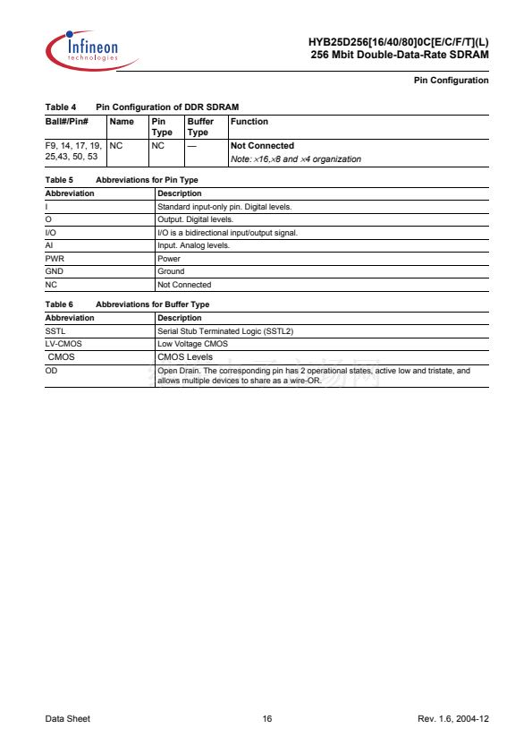
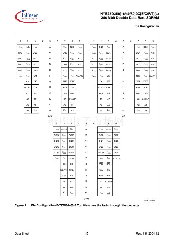
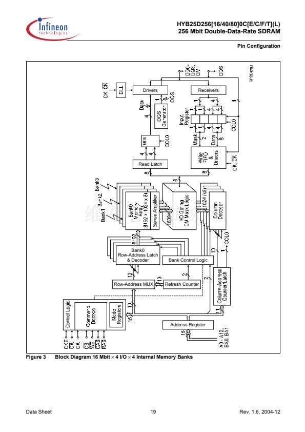
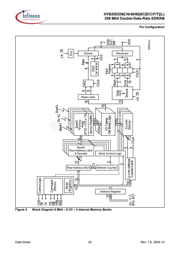
鈩?/div>
limits the input current from the
V
TT
supply into any pin and
V
REF
tracks
V
DDQ
/2
or the following relationship must be followed:
V
DDQ
is driven after or with
V
DD
such that
V
DDQ
<
V
DD
+ 0.3 V
V
TT
is driven after or with
V
DDQ
such that
V
TT
<
V
DDQ
+ 0.3 V
V
REF
is driven after or with
V
DDQ
such that
V
REF
<
V
DDQ
+ 0.3 V
V
DD
and
V
DDQ
are driven from a single power converter output
V
TT
meets the specification
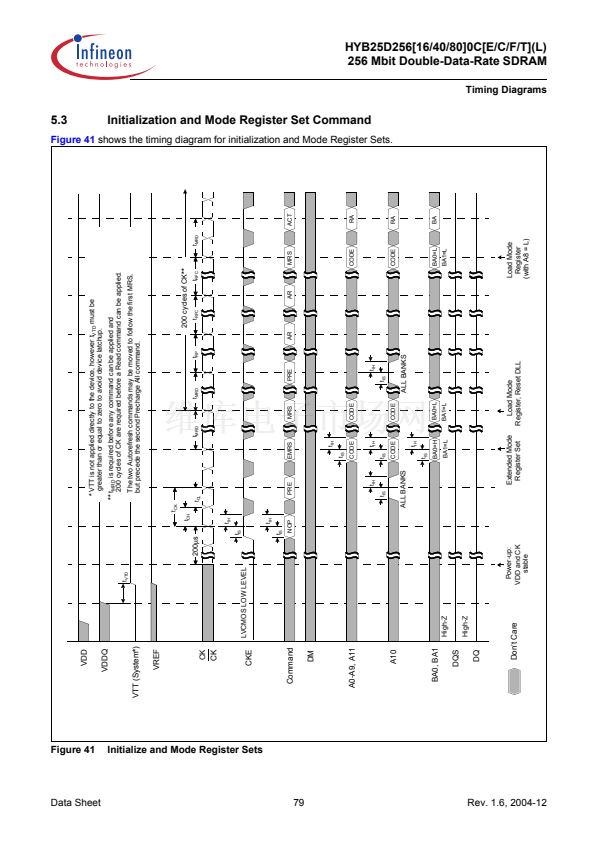
The DQ and DQS outputs are in the High-Z state, where they remain until driven in normal operation (by a read
access). After all power supply and reference voltages are stable, and the clock is stable, the DDR SDRAM
requires a 200
碌s
delay prior to applying an executable command.
Once the 200
碌s
delay has been satisfied, a Deselect or NOP command should be applied, and CKE should be
brought HIGH. Following the NOP command, a Precharge ALL command should be applied. Next a Mode
Register Set command should be issued for the Extended Mode Register, to enable the DLL, then a Mode
Register Set command should be issued for the Mode Register, to reset the DLL, and to program the operating
parameters. 200 clock cycles are required between the DLL reset and any executable command. During the
200 cycles of clock for DLL locking, a Deselect or NOP command must be applied. After the 200 clock cycles, a
Precharge ALL command should be applied, placing the device in the 鈥渁ll banks idle鈥?state.
Once in the idle state, two AUTO REFRESH cycles must be performed. Additionally, a Mode Register Set
command for the Mode Register, with the reset DLL bit deactivated (i.e. to program operating parameters without
resetting the DLL) must be performed. Following these cycles, the DDR SDRAM is ready for normal operation.
Data Sheet
22
Rev. 1.6, 2004-12


 1
1
 2
2
 3
3
 4
4
 5
5
 6
6
 7
7
 8
8
 9
9
 10
10
 11
11
 12
12
 13
13
 14
14
 15
15
 16
16
 17
17
 18
18
 19
19
 20
20
 21
21
 22
22
 23
23
 24
24
 25
25
 26
26
 27
27
 28
28
 29
29
 30
30
 31
31
 32
32
 33
33
 34
34
 35
35
 36
36
 37
37
 38
38
 39
39
 40
40
 41
41
 42
42
 43
43
 44
44
 45
45
 46
46
 47
47
 48
48
 49
49
 50
50
 51
51
 52
52
 53
53
 54
54
 55
55
 56
56
 57
57
 58
58
 59
59
 60
60
 61
61
 62
62
 63
63
 64
64
 65
65
 66
66
 67
67
 68
68
 69
69
 70
70
 71
71
 72
72
 73
73
 74
74
 75
75
 76
76
 77
77
 78
78
 79
79
 80
80
 81
81
 82
82
 83
83
 84
84
 85
85
 86
86
 87
87
 88
88
 89
89
 90
90
 91
91
 92
92
 93
93
 94
94
