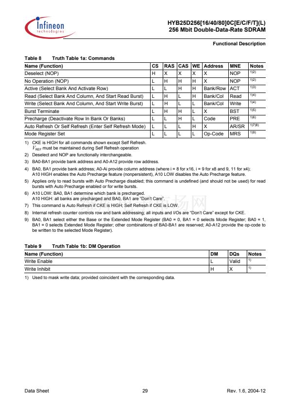
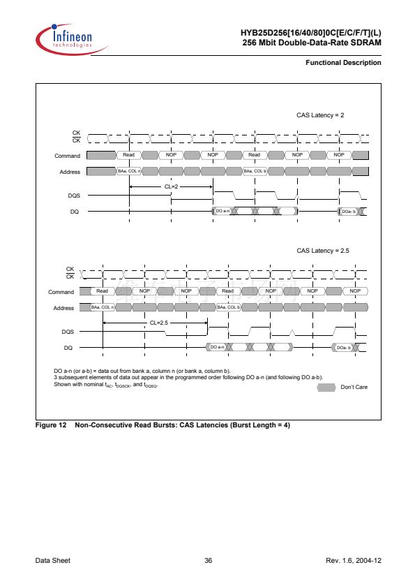
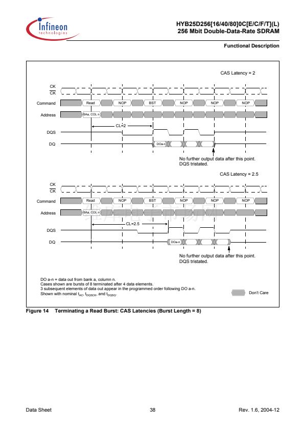
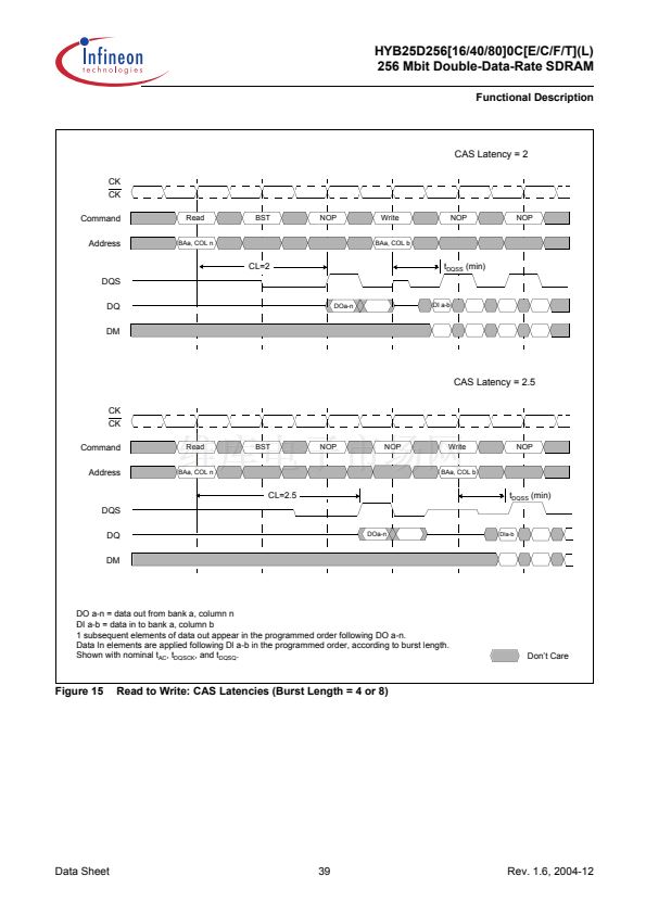
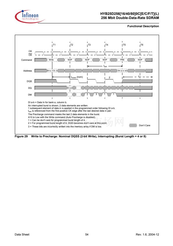
HYB25D256[16/40/80]0C[E/C/F/T](L)
256 Mbit Double-Data-Rate SDRAM
Functional Description
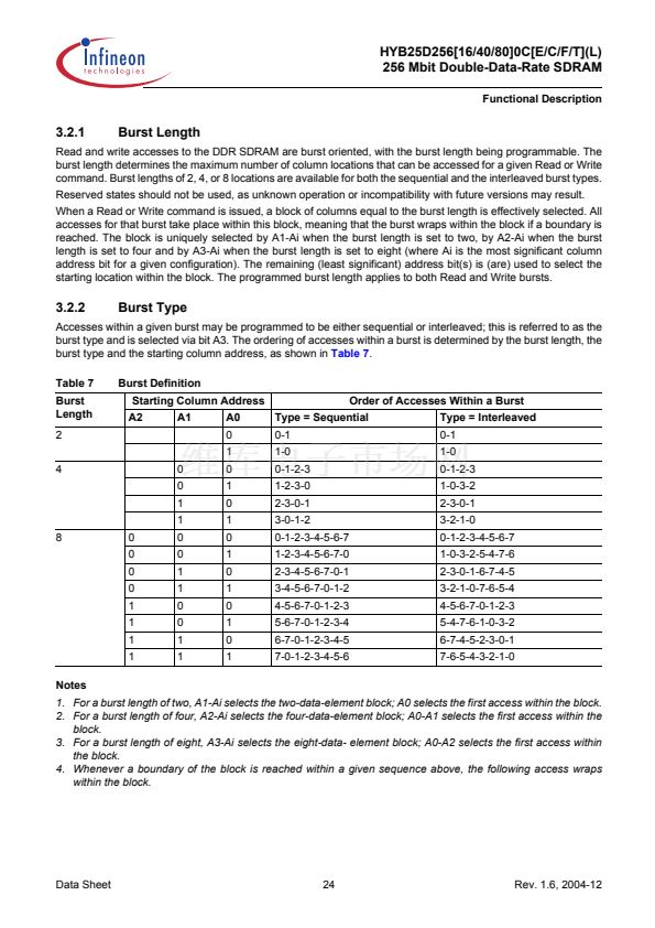
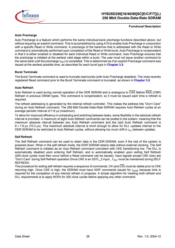
3.5
3.5.1
Operations
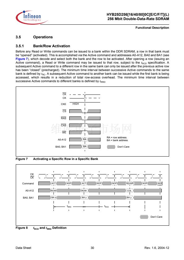
Bank/Row Activation
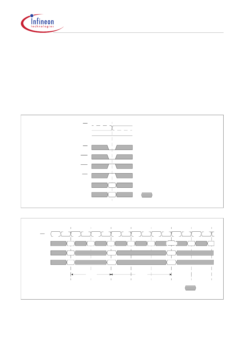
Before any Read or Write commands can be issued to a bank within the DDR SDRAM, a row in that bank must
be 鈥渙pened鈥?(activated). This is accomplished via the Active command and addresses A0-A12, BA0 and BA1 (see
Figure 7),
which decode and select both the bank and the row to be activated. After opening a row (issuing an
Active command), a Read or Write command may be issued to that row, subject to the
t
RCD
specification. A
subsequent Active command to a different row in the same bank can only be issued after the previous active row
has been 鈥渃losed鈥?(precharged). The minimum time interval between successive Active commands to the same
bank is defined by
t
RC
. A subsequent Active command to another bank can be issued while the first bank is being
accessed, which results in a reduction of total row-access overhead. The minimum time interval between
successive Active commands to different banks is defined by
t
RRD
.
CK
CK
CKE
CS
RAS
CAS
WE
A0-A12
BA0, BA1
RA
BA
RA = row address.
BA = bank address.
Don鈥檛 Care
HIGH
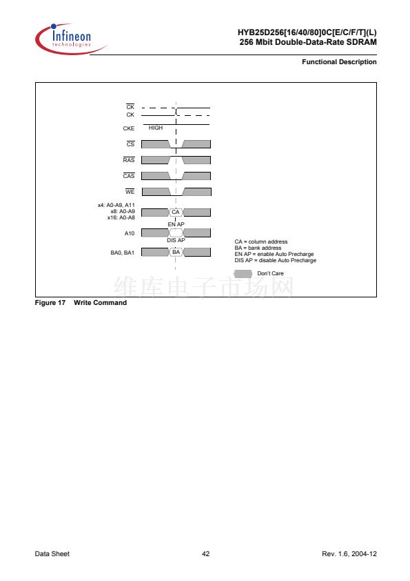
Figure 7
Activating a Specific Row in a Specific Bank
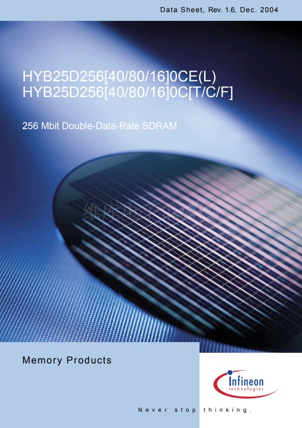
CK
CK
Command
A0-A12
BA0, BA1
ACT
ROW
BA x
NOP
ACT
ROW
BA y
NOP
NOP
RD/WR
COL
BA y
NOP
NOP
t
RRD
t
RCD
Don鈥檛 Care
Figure 8
t
RCD
and
t
RRD
Definition
Data Sheet
30
Rev. 1.6, 2004-12


 1
1
 2
2
 3
3
 4
4
 5
5
 6
6
 7
7
 8
8
 9
9
 10
10
 11
11
 12
12
 13
13
 14
14
 15
15
 16
16
 17
17
 18
18
 19
19
 20
20
 21
21
 22
22
 23
23
 24
24
 25
25
 26
26
 27
27
 28
28
 29
29
 30
30
 31
31
 32
32
 33
33
 34
34
 35
35
 36
36
 37
37
 38
38
 39
39
 40
40
 41
41
 42
42
 43
43
 44
44
 45
45
 46
46
 47
47
 48
48
 49
49
 50
50
 51
51
 52
52
 53
53
 54
54
 55
55
 56
56
 57
57
 58
58
 59
59
 60
60
 61
61
 62
62
 63
63
 64
64
 65
65
 66
66
 67
67
 68
68
 69
69
 70
70
 71
71
 72
72
 73
73
 74
74
 75
75
 76
76
 77
77
 78
78
 79
79
 80
80
 81
81
 82
82
 83
83
 84
84
 85
85
 86
86
 87
87
 88
88
 89
89
 90
90
 91
91
 92
92
 93
93
 94
94
