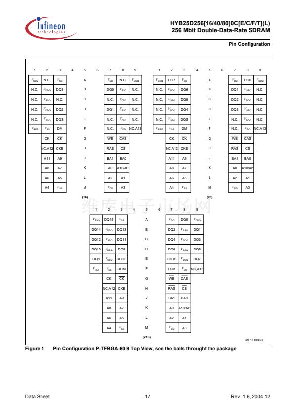
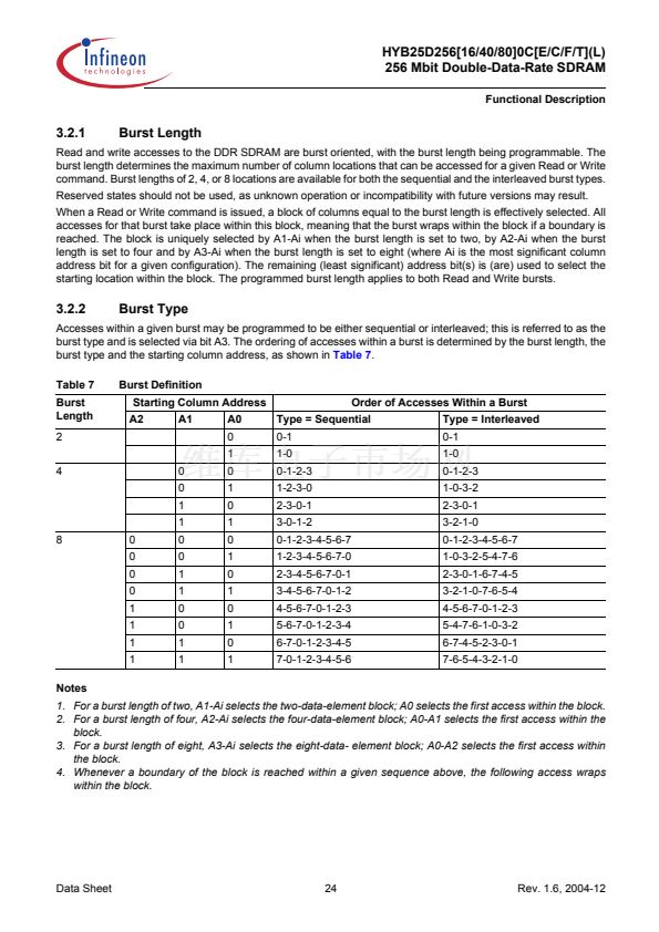
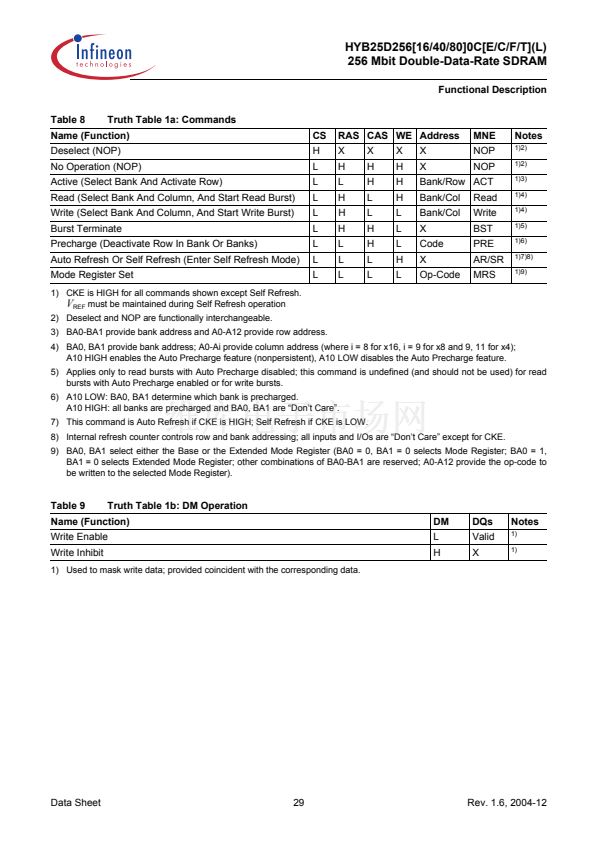
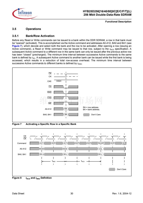
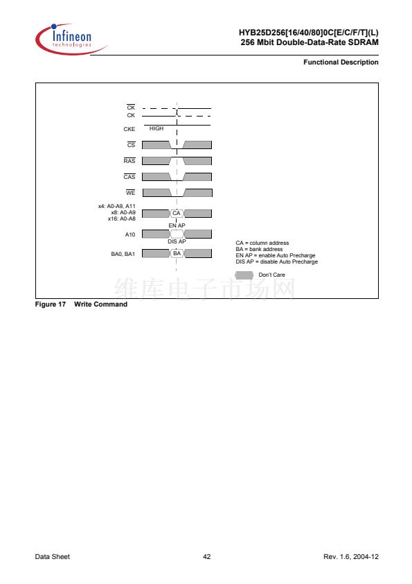
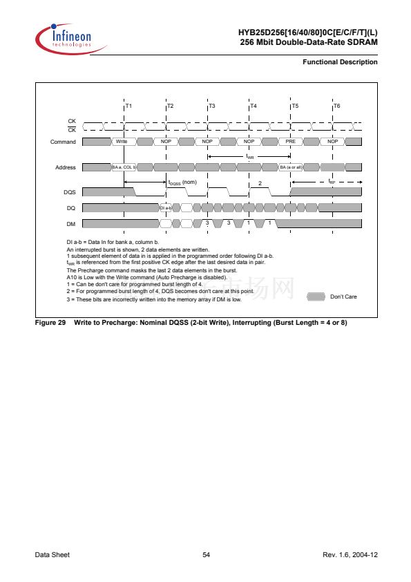
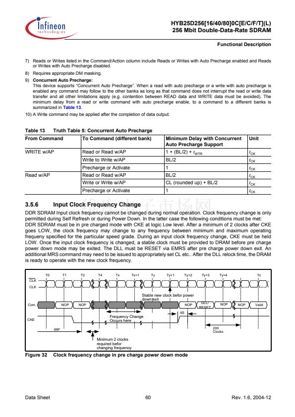
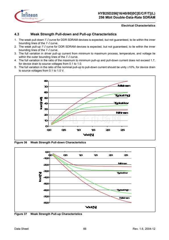
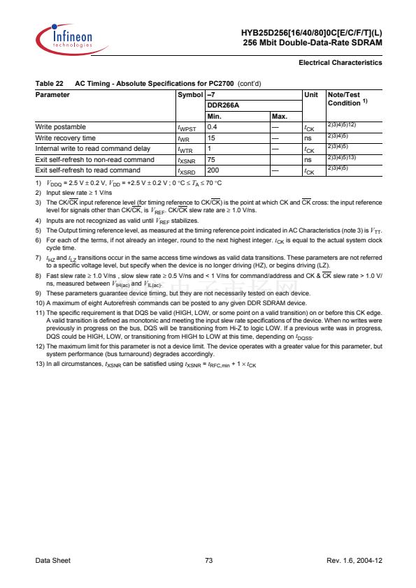
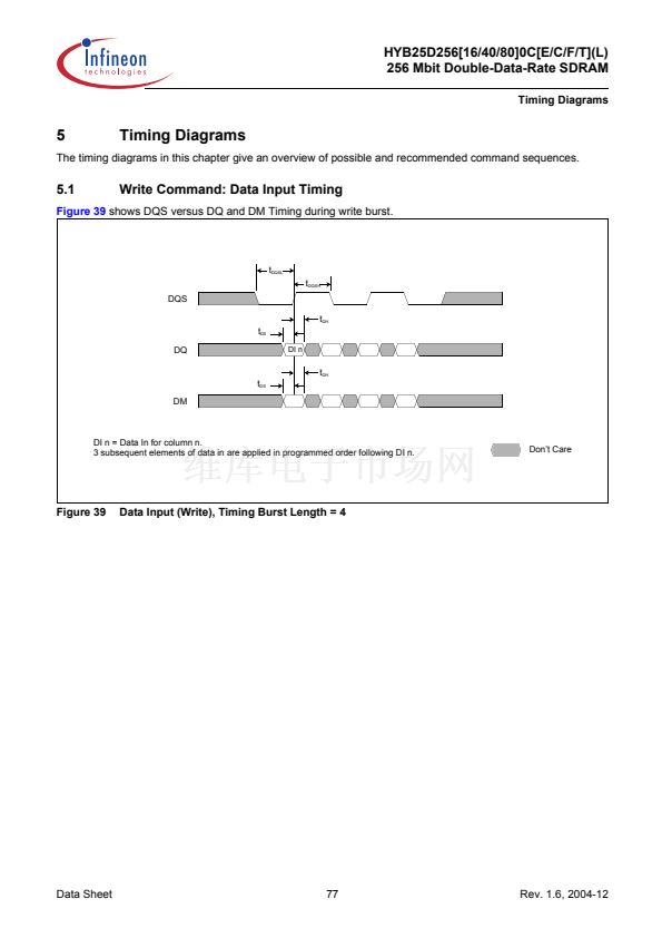
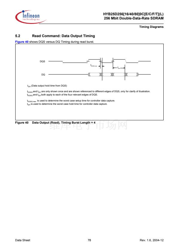
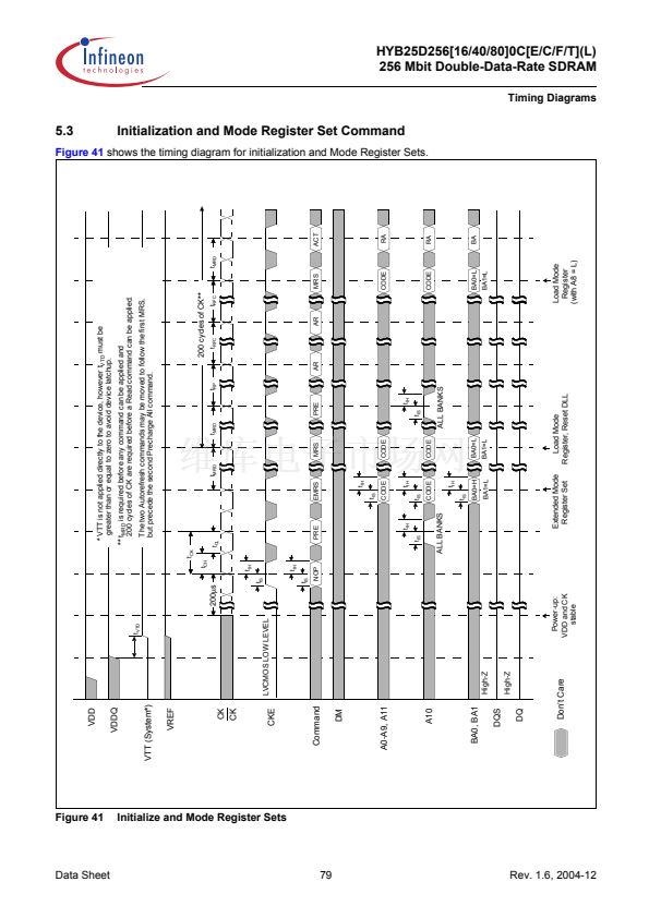
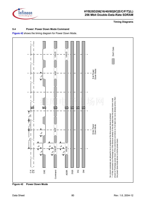
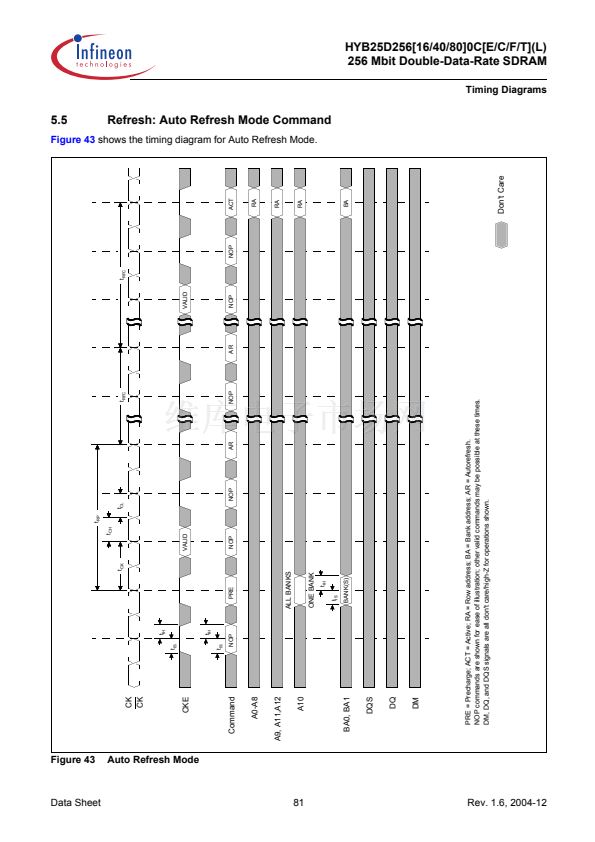
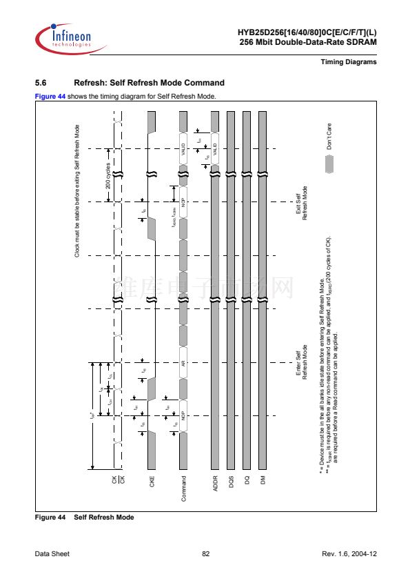
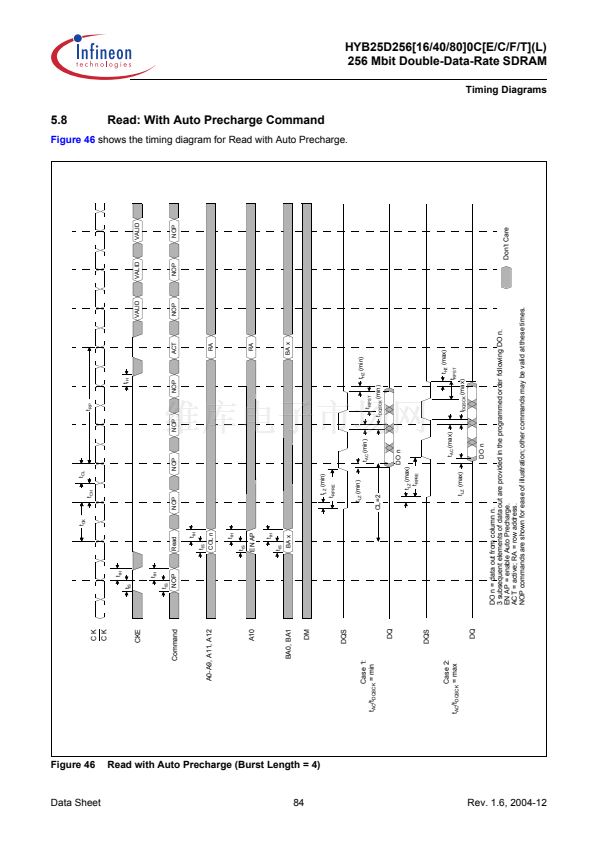
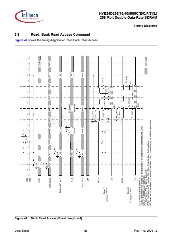
HYB25D256[16/40/80]0C[E/C/F/T](L)
256 Mbit Double-Data-Rate SDRAM
Electrical Characteristics
4.4
AC Characteristics
(Notes 1-5 apply to the following Tables; Electrical Characteristics and DC Operating Conditions, AC Operating
Conditions,
I
DD
Specifications and Conditions, and Electrical Characteristics and AC Timing.)
Notes
1. All voltages referenced to
V
SS
.
2. Tests for AC timing,
I
DD
, and electrical, AC and DC characteristics, may be conducted at nominal reference/
supply voltage levels, but the related specifications and device operation are guaranteed for the full voltage
range specified.
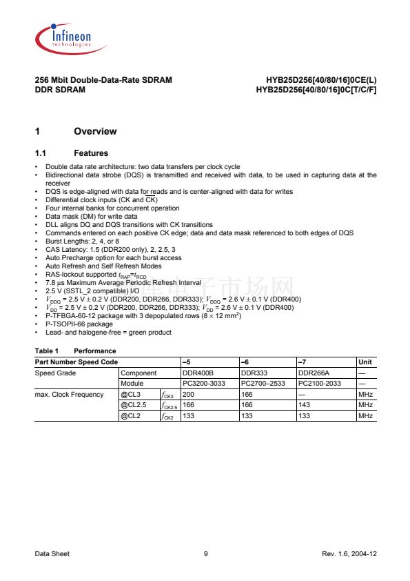
3.
Figure 38
represents the timing reference load used in defining the relevant timing parameters of the part. It
is not intended to be either a precise representation of the typical system environment nor a depiction of the
actual load presented by a production tester. System designers will use IBIS or other simulation tools to
correlate the timing reference load to a system environment. Manufacturers will correlate to their production
test conditions (generally a coaxial transmission line terminated at the tester electronics).
4. AC timing and
I
DD
tests may use a
V
IL
to
V
IH
swing of up to 1.5 V in the test environment, but input timing is
still referenced to
V
REF
(or to the crossing point for CK, CK), and parameter specifications are guaranteed for
the specified AC input levels under normal use conditions. The minimum slew rate for the input signals is 1 V/
ns in the range between
V
IL(AC)
and
V
IH(AC)
.
5. The AC and DC input level specifications are as defined in the SSTL_2 Standard (i.e. the receiver effectively
switches as a result of the signal crossing the AC input level, and remains in that state as long as the signal
does not ring back above (below) the DC input LOW (HIGH) level).
6. For System Characteristics like Setup & Holdtime Derating for Slew Rate, I/O Delta Rise/Fall Derating, DDR
SDRAM Slew Rate Standards, Overshoot & Undershoot specification and Clamp
V
-
I
characteristics see the
latest JEDEC specification for DDR components.
V
TT
50
鈩?/div>
Output
(
V
OUT
)
Timing Reference Point
30 pF
Figure 38
AC Output Load Circuit Diagram / Timing Reference Load
Data Sheet
68
Rev. 1.6, 2004-12


 1
1
 2
2
 3
3
 4
4
 5
5
 6
6
 7
7
 8
8
 9
9
 10
10
 11
11
 12
12
 13
13
 14
14
 15
15
 16
16
 17
17
 18
18
 19
19
 20
20
 21
21
 22
22
 23
23
 24
24
 25
25
 26
26
 27
27
 28
28
 29
29
 30
30
 31
31
 32
32
 33
33
 34
34
 35
35
 36
36
 37
37
 38
38
 39
39
 40
40
 41
41
 42
42
 43
43
 44
44
 45
45
 46
46
 47
47
 48
48
 49
49
 50
50
 51
51
 52
52
 53
53
 54
54
 55
55
 56
56
 57
57
 58
58
 59
59
 60
60
 61
61
 62
62
 63
63
 64
64
 65
65
 66
66
 67
67
 68
68
 69
69
 70
70
 71
71
 72
72
 73
73
 74
74
 75
75
 76
76
 77
77
 78
78
 79
79
 80
80
 81
81
 82
82
 83
83
 84
84
 85
85
 86
86
 87
87
 88
88
 89
89
 90
90
 91
91
 92
92
 93
93
 94
94
