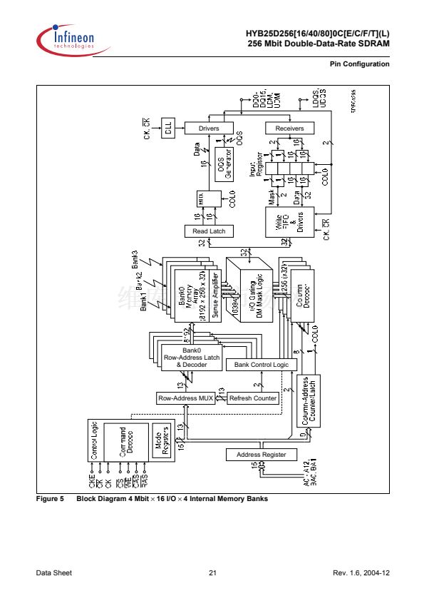
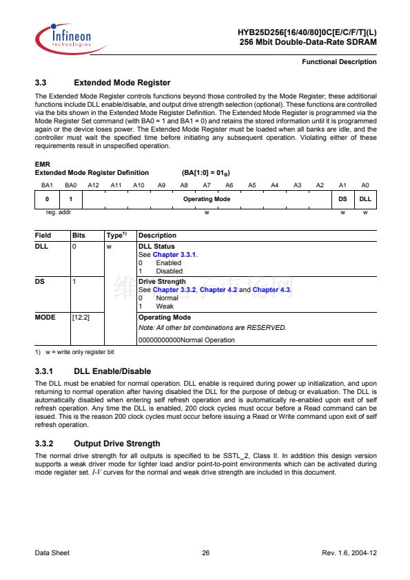
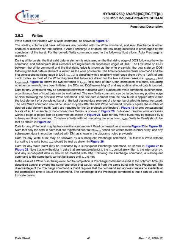
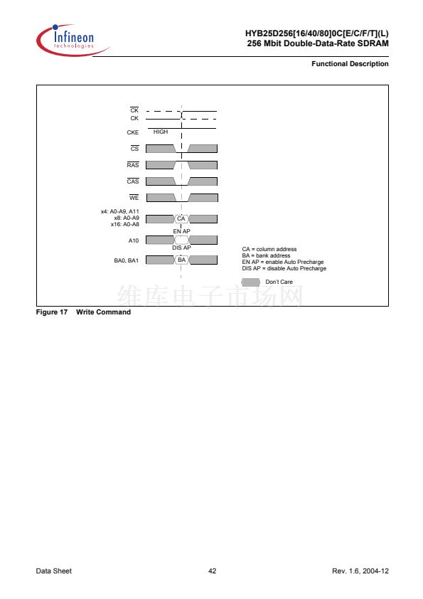
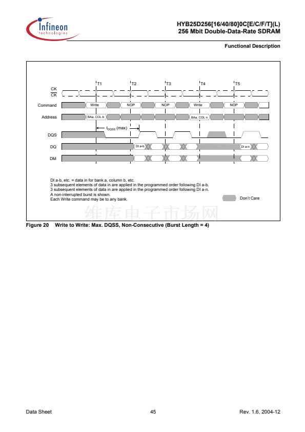
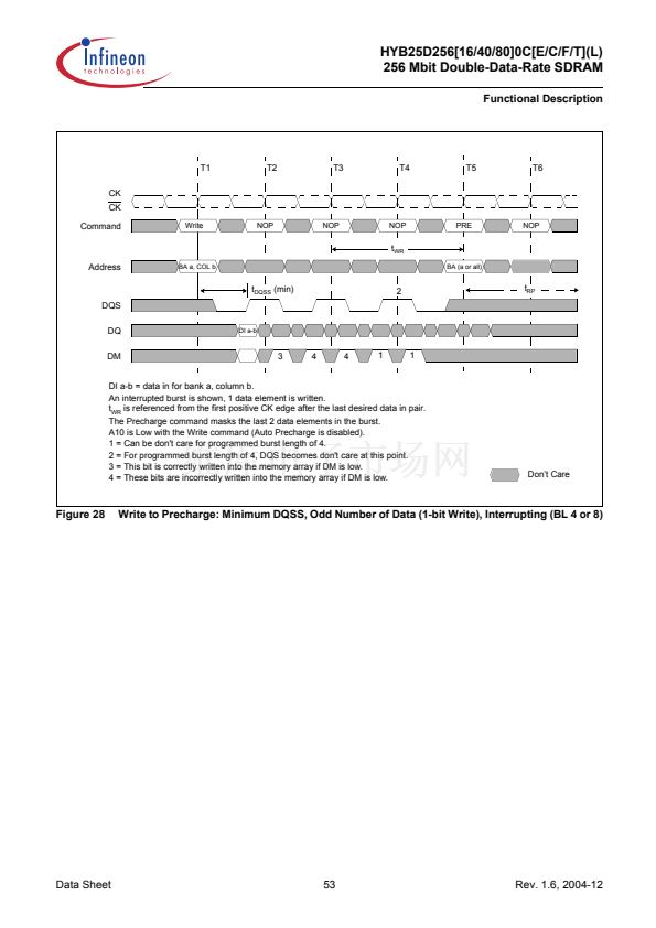
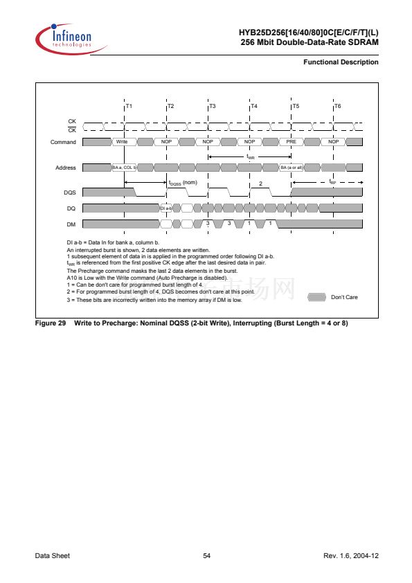
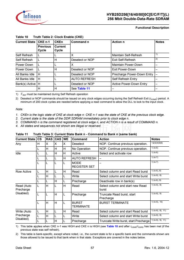
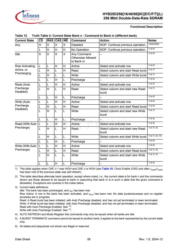
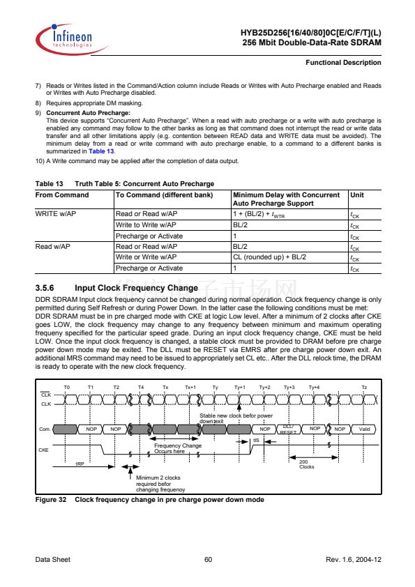
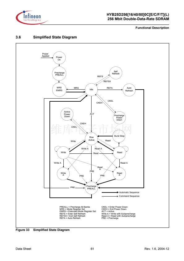
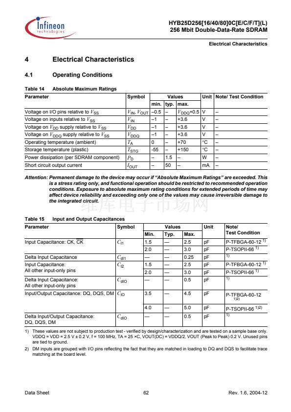
鈮?/div>
70
掳C
2) Input slew rate = 1 V/ns.
3) Inputs are not recognized as valid until
V
REF
stabilizes.
4)
V
ID
is the magnitude of the difference between the input level on CK and the input level on CK.
5) The value of
V
IX
is expected to equal 0.5
脳
V
DDQ
of the transmitting device and must track variations in the DC level of the
same.
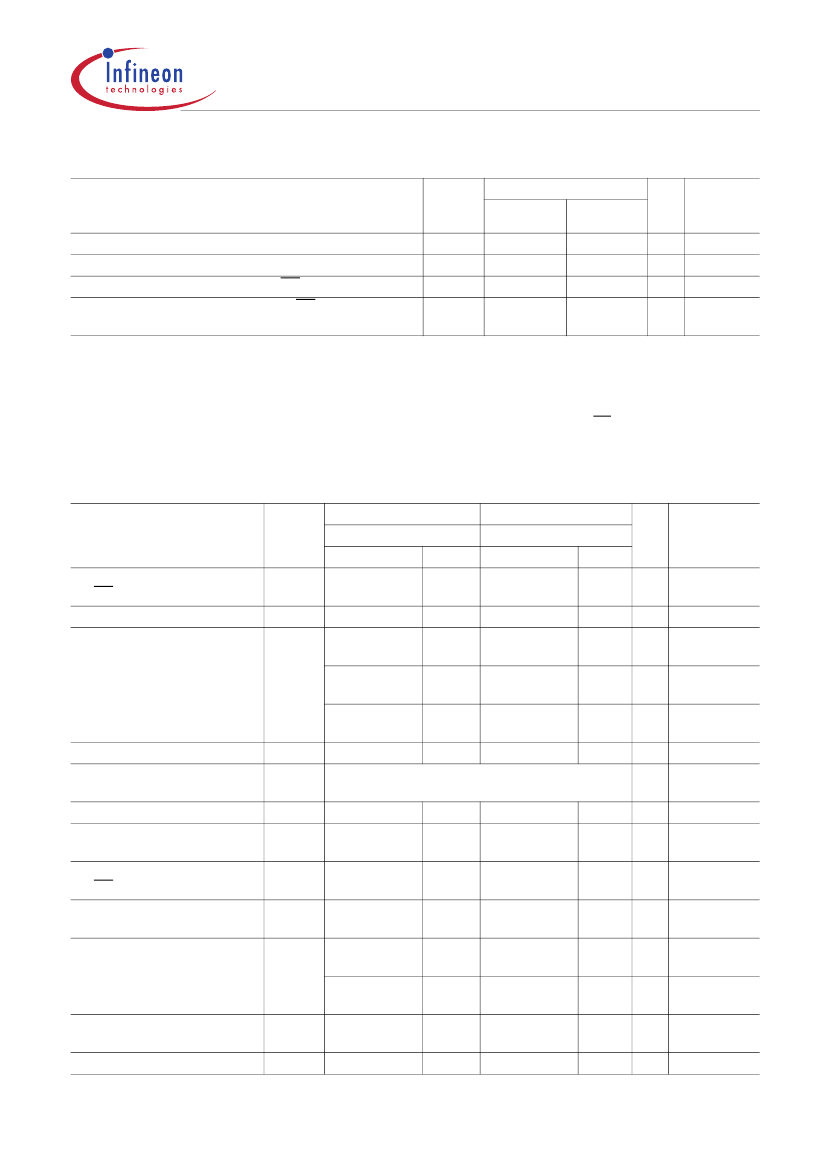
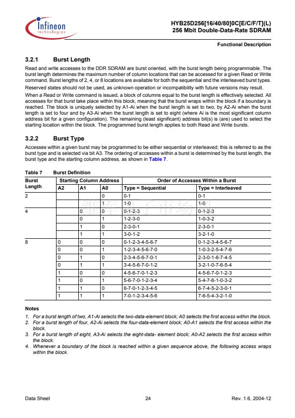
Table 21
Parameter
AC Timing - Absolute Specifications for PC3200 and PC2700
Symbol 鈥?
DDR400B
Min.
Max.
+0.5
0.55
8
12
12
0.55
鈥?
DDR333
Min.
鈥?.7
0.45
6
6
7.5
0.45
Max.
+0.7
0.55
12
12
12
0.55
ns
2)3)4)5)
2)3)4)5)
Unit Note/ Test
Condition
1)
DQ output access time from
CK/CK
CK high-level width
Clock cycle time
t
AC
t
CH
t
CK
鈥?.5
0.45
5
6
7.5
t
CK
ns
ns
ns
CL = 3.0
2)3)4)5)
2)3)4)5)
2)3)4)5)
CL = 2.5
CL = 2.0
t
CL
Auto precharge write recovery
t
DAL
CK low-level width
+ precharge time
DQ and DM input hold time
DQ and DM input pulse width
(each input)
DQS output access time from
CK/CK
DQS input low (high) pulse
width (write cycle)
DQS-DQ skew (DQS and
associated DQ signals)
0.45
(
t
WR
/
t
CK
)+(
t
RP
/
t
CK
)
0.4
1.75
鈥?.6
鈥?/div>
鈥?/div>
+0.6
鈥?/div>
+0.40
+0.40
1.25
鈥?/div>
0.45
1.75
鈥?.6
0.35
鈥?/div>
鈥?/div>
0.75
0.45
鈥?/div>
鈥?/div>
+0.6
鈥?/div>
+0.40
+0.45
1.25
鈥?/div>
t
CK
t
CK
ns
ns
ns
2)3)4)5)
2)3)4)5)6)
2)3)4)5)
2)3)4)5)6)
2)3)4)5)
2)3)4)5)
t
DH
t
DIPW
t
DQSCK
t
DQSL,H
0.35
t
DQSQ
鈥?/div>
鈥?/div>
t
CK
ns
ns
2)3)4)5)
2)3)4)5)
TFBGA
TSOPII
Write command to 1
st
DQS
latching transition
DQ and DM input setup time
t
DQSS
t
DS
0.72
0.4
t
CK
ns
2)3)4)5)
2)3)4)5)
Data Sheet
69
Rev. 1.6, 2004-12
HYB25D256800CL-6相关型号PDF文件下载
-
型号
版本
描述
厂商
下载
-
英文版
128-Mbit Double-Data-Rate SDRAM
QIMONDA [Q...
-
英文版
128 Mbit DDR SGRAM
INFINEON [...
-
英文版
128-Mbit Double-Data-Rate SDRAM
QIMONDA [Q...
-
英文版
128-Mbit Double-Data-Rate SDRAM
QIMONDA [Q...
-
英文版
256 Mbit Double Data Rate SDRAM
INFINEON [...
-
英文版
Qimonda AG [DDR SDRAM]
-
英文版
DDR SDRAM
QIMONDA [Qimond...
-
英文版
128 Mbit Double Data Rate SDRAM
-
英文版
128 Mbit Double Data Rate SDRAM
INFINEON [...
-
英文版
128 Mbit Double Data Rate SDRAM
INFINEON [...
-
英文版
MEMORY SPECTRUM
INFINEON [...
-
英文版
16M x 16 Double Data Rate Graphics DRAM
INFINEON [...
-
英文版
256-Mbit Double Data Rate SDRAM, Die Rev. B
INFINEON [...
-
英文版
256MBit Double Data Rata SDRAM
INFINEON [...
-
英文版
Qimonda AG [256-Mbit Double-Data-Rate SDRAM]
-
英文版
512Mbit Double Data Rate SDRAM
-
英文版
512Mbit Double Data Rate SDRAM
INFINEON [...
-
英文版
512Mbit Double Data Rate SDRAM
-
英文版
512Mbit Double Data Rate SDRAM
INFINEON [...
-
英文版
512Mbit Double Data Rate SDRAM
INFINEON [...


 1
1
 2
2
 3
3
 4
4
 5
5
 6
6
 7
7
 8
8
 9
9
 10
10
 11
11
 12
12
 13
13
 14
14
 15
15
 16
16
 17
17
 18
18
 19
19
 20
20
 21
21
 22
22
 23
23
 24
24
 25
25
 26
26
 27
27
 28
28
 29
29
 30
30
 31
31
 32
32
 33
33
 34
34
 35
35
 36
36
 37
37
 38
38
 39
39
 40
40
 41
41
 42
42
 43
43
 44
44
 45
45
 46
46
 47
47
 48
48
 49
49
 50
50
 51
51
 52
52
 53
53
 54
54
 55
55
 56
56
 57
57
 58
58
 59
59
 60
60
 61
61
 62
62
 63
63
 64
64
 65
65
 66
66
 67
67
 68
68
 69
69
 70
70
 71
71
 72
72
 73
73
 74
74
 75
75
 76
76
 77
77
 78
78
 79
79
 80
80
 81
81
 82
82
 83
83
 84
84
 85
85
 86
86
 87
87
 88
88
 89
89
 90
90
 91
91
 92
92
 93
93
 94
94
