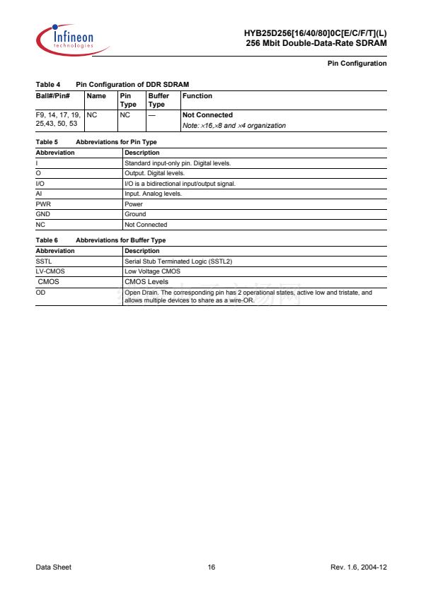
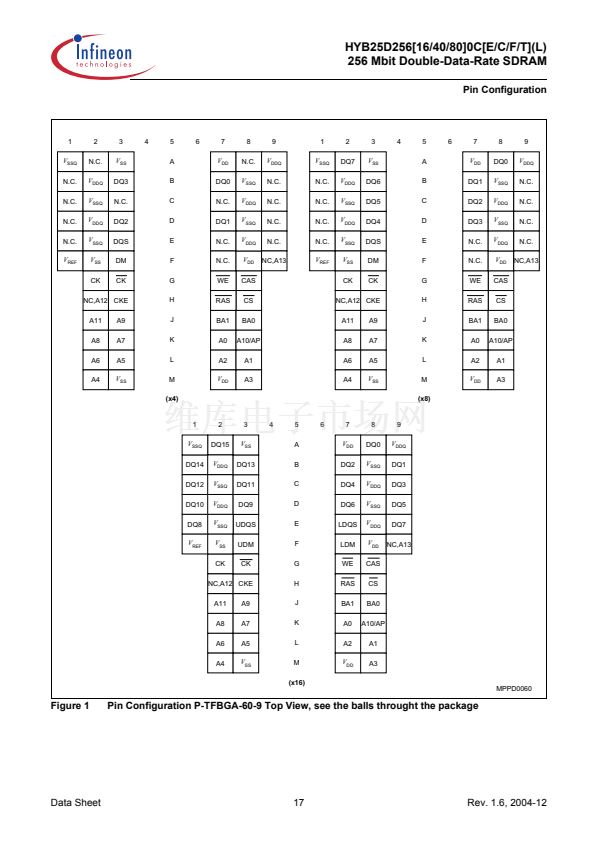
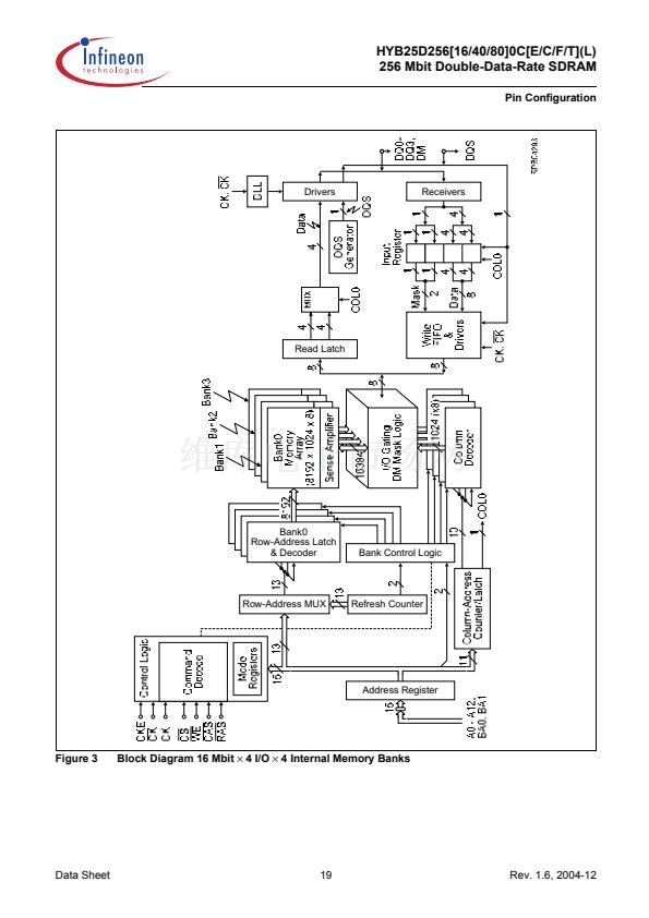
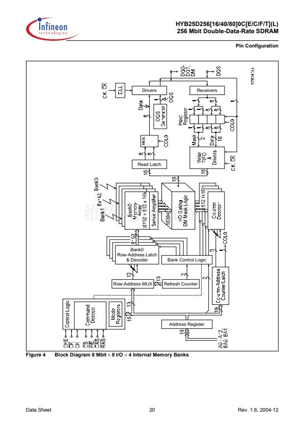
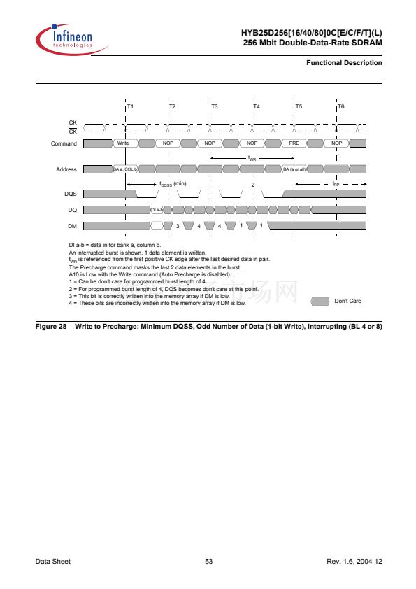
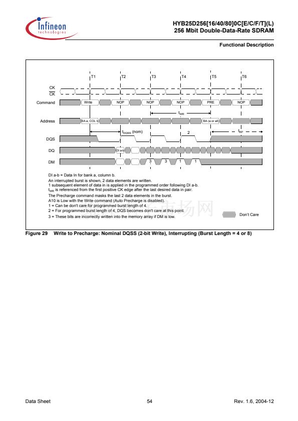
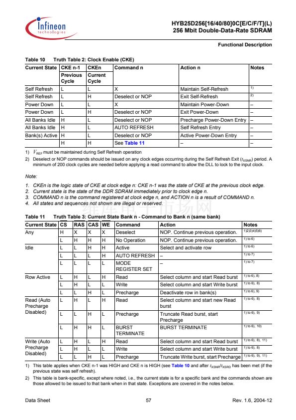
鈮?/div>
0.5 V/ns and < 1 V/ns for command/address and CK & CK slew rate > 1.0 V/
ns, measured between
V
IH(ac)
and
V
IL(ac)
.
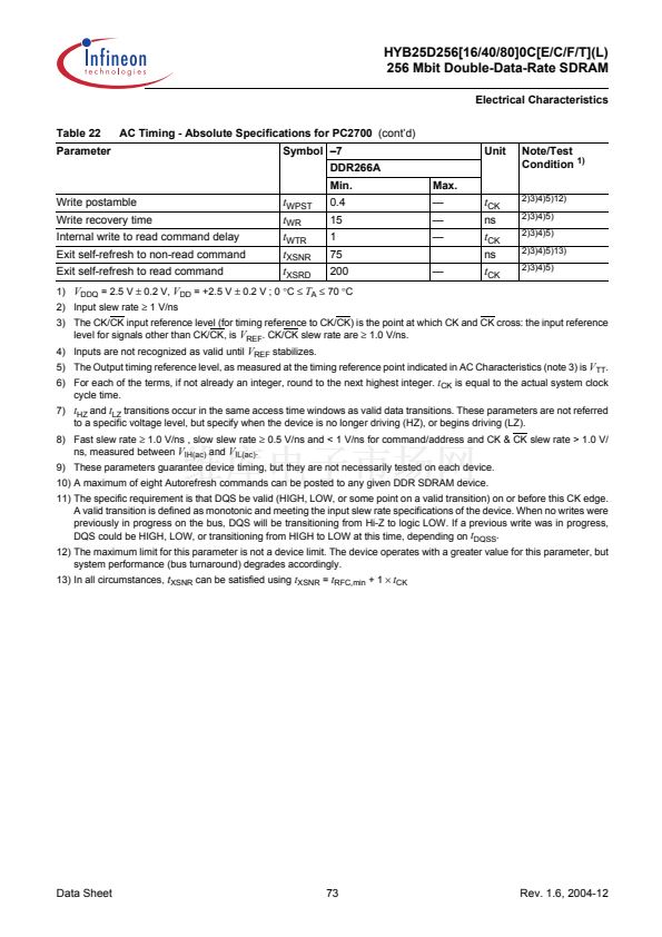
9) These parameters guarantee device timing, but they are not necessarily tested on each device.
10) A maximum of eight Autorefresh commands can be posted to any given DDR SDRAM device.
11) The specific requirement is that DQS be valid (HIGH, LOW, or some point on a valid transition) on or before this CK edge.
A valid transition is defined as monotonic and meeting the input slew rate specifications of the device. When no writes were
previously in progress on the bus, DQS will be transitioning from Hi-Z to logic LOW. If a previous write was in progress,
DQS could be HIGH, LOW, or transitioning from HIGH to LOW at this time, depending on
t
DQSS
.
12) The maximum limit for this parameter is not a device limit. The device operates with a greater value for this parameter, but
system performance (bus turnaround) degrades accordingly.
13) In all circumstances,
t
XSNR
can be satisfied using
t
XSNR
=
t
RFC,min
+ 1
脳
t
CK
Unit
Max.
鈥?/div>
鈥?/div>
鈥?/div>
鈥?/div>
Note/Test
Condition
1)
2)3)4)5)12)
2)3)4)5)
2)3)4)5)
2)3)4)5)13)
2)3)4)5)
t
WPST
t
WR
t
WTR
t
XSNR
t
XSRD
0.4
15
1
75
200
t
CK
ns
t
CK
ns
t
CK
1)
V
DDQ
= 2.5 V
卤
0.2 V,
V
DD
= +2.5 V
卤
0.2 V ; 0
掳C 鈮?/div>
T
A
鈮?/div>
70
掳C
Data Sheet
73
Rev. 1.6, 2004-12
HYB25D256800CL-6相关型号PDF文件下载
-
型号
版本
描述
厂商
下载
-
英文版
128-Mbit Double-Data-Rate SDRAM
QIMONDA [Q...
-
英文版
128 Mbit DDR SGRAM
INFINEON [...
-
英文版
128-Mbit Double-Data-Rate SDRAM
QIMONDA [Q...
-
英文版
128-Mbit Double-Data-Rate SDRAM
QIMONDA [Q...
-
英文版
256 Mbit Double Data Rate SDRAM
INFINEON [...
-
英文版
Qimonda AG [DDR SDRAM]
-
英文版
DDR SDRAM
QIMONDA [Qimond...
-
英文版
128 Mbit Double Data Rate SDRAM
-
英文版
128 Mbit Double Data Rate SDRAM
INFINEON [...
-
英文版
128 Mbit Double Data Rate SDRAM
INFINEON [...
-
英文版
MEMORY SPECTRUM
INFINEON [...
-
英文版
16M x 16 Double Data Rate Graphics DRAM
INFINEON [...
-
英文版
256-Mbit Double Data Rate SDRAM, Die Rev. B
INFINEON [...
-
英文版
256MBit Double Data Rata SDRAM
INFINEON [...
-
英文版
Qimonda AG [256-Mbit Double-Data-Rate SDRAM]
-
英文版
512Mbit Double Data Rate SDRAM
-
英文版
512Mbit Double Data Rate SDRAM
INFINEON [...
-
英文版
512Mbit Double Data Rate SDRAM
-
英文版
512Mbit Double Data Rate SDRAM
INFINEON [...
-
英文版
512Mbit Double Data Rate SDRAM
INFINEON [...


 1
1
 2
2
 3
3
 4
4
 5
5
 6
6
 7
7
 8
8
 9
9
 10
10
 11
11
 12
12
 13
13
 14
14
 15
15
 16
16
 17
17
 18
18
 19
19
 20
20
 21
21
 22
22
 23
23
 24
24
 25
25
 26
26
 27
27
 28
28
 29
29
 30
30
 31
31
 32
32
 33
33
 34
34
 35
35
 36
36
 37
37
 38
38
 39
39
 40
40
 41
41
 42
42
 43
43
 44
44
 45
45
 46
46
 47
47
 48
48
 49
49
 50
50
 51
51
 52
52
 53
53
 54
54
 55
55
 56
56
 57
57
 58
58
 59
59
 60
60
 61
61
 62
62
 63
63
 64
64
 65
65
 66
66
 67
67
 68
68
 69
69
 70
70
 71
71
 72
72
 73
73
 74
74
 75
75
 76
76
 77
77
 78
78
 79
79
 80
80
 81
81
 82
82
 83
83
 84
84
 85
85
 86
86
 87
87
 88
88
 89
89
 90
90
 91
91
 92
92
 93
93
 94
94
