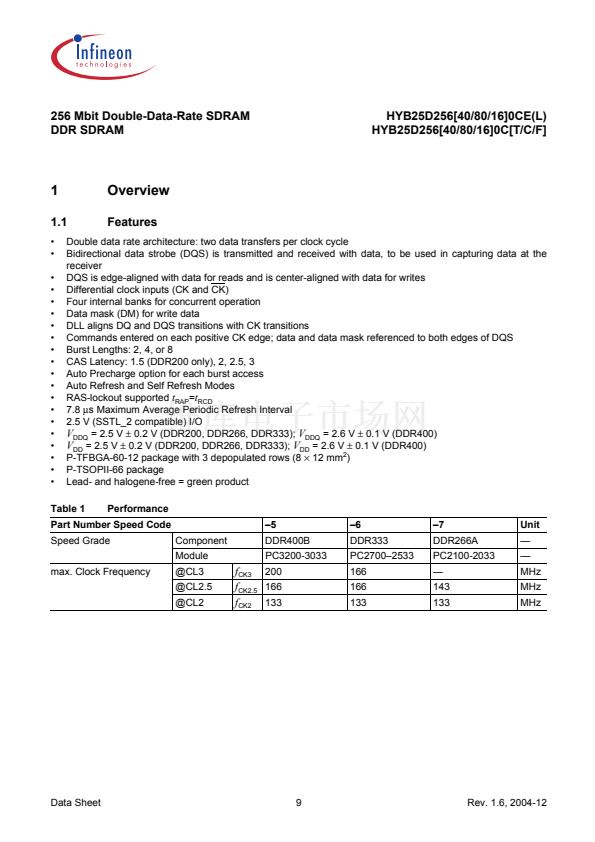
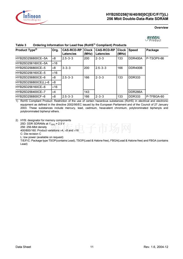
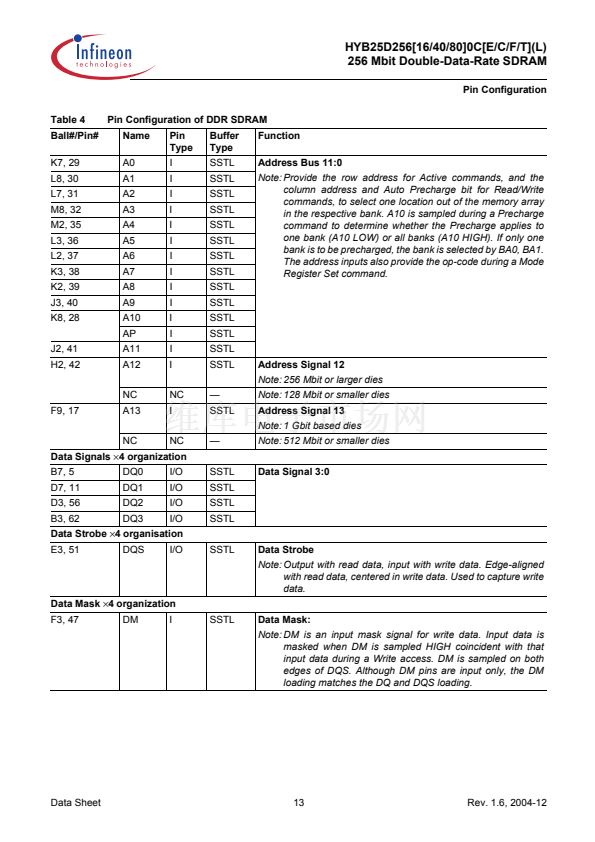
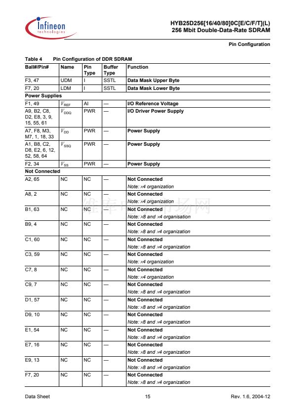
鈮?/div>
V
IHMIN
;
t
RC
=
t
RASMAX
;
t
CK
=
t
CKMIN
;
I
DD3N
DQ, DM and DQS inputs changing twice per clock cycle; address and control inputs changing once per
clock cycle.
Operating Current:
one bank active; Burst = 2; reads; continuous burst; address and control inputs
I
DD4R
changing once per clock cycle; 50% of data outputs changing on every clock edge; CL = 2 for DDR200
and DDR266A, CL = 3 for DDR333;
t
CK
=
t
CKMIN
;
I
OUT
= 0 mA
Operating Current:
one bank active; Burst = 2; writes; continuous burst; address and control inputs
I
DD4W
changing once per clock cycle; 50% of data outputs changing on every clock edge; CL = 2 for DDR200
and DDR266A, CL = 3 for DDR333;
t
CK
=
t
CKMIN
Auto-Refresh Current:
t
RC
=
t
RFCMIN
, burst refresh
Self-Refresh Current:
CKE
鈮?/div>
0.2 V; external clock on;
t
CK
=
t
CKMIN
Operating Current:
four bank; four bank interleaving with BL = 4; Refer to the following page for
detailed test conditions.
I
DD5
I
DD6
I
DD7
Data Sheet
74
Rev. 1.6, 2004-12


 1
1
 2
2
 3
3
 4
4
 5
5
 6
6
 7
7
 8
8
 9
9
 10
10
 11
11
 12
12
 13
13
 14
14
 15
15
 16
16
 17
17
 18
18
 19
19
 20
20
 21
21
 22
22
 23
23
 24
24
 25
25
 26
26
 27
27
 28
28
 29
29
 30
30
 31
31
 32
32
 33
33
 34
34
 35
35
 36
36
 37
37
 38
38
 39
39
 40
40
 41
41
 42
42
 43
43
 44
44
 45
45
 46
46
 47
47
 48
48
 49
49
 50
50
 51
51
 52
52
 53
53
 54
54
 55
55
 56
56
 57
57
 58
58
 59
59
 60
60
 61
61
 62
62
 63
63
 64
64
 65
65
 66
66
 67
67
 68
68
 69
69
 70
70
 71
71
 72
72
 73
73
 74
74
 75
75
 76
76
 77
77
 78
78
 79
79
 80
80
 81
81
 82
82
 83
83
 84
84
 85
85
 86
86
 87
87
 88
88
 89
89
 90
90
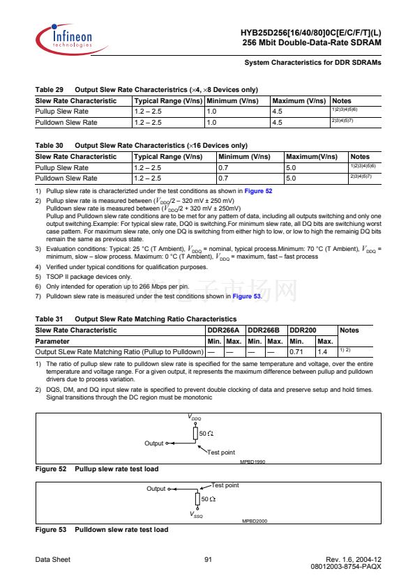 91
91
 92
92
 93
93
 94
94
