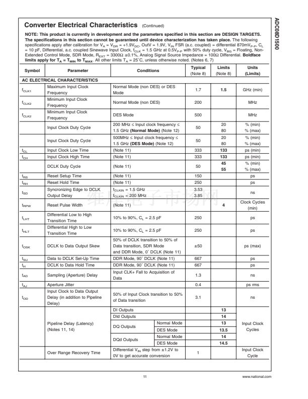
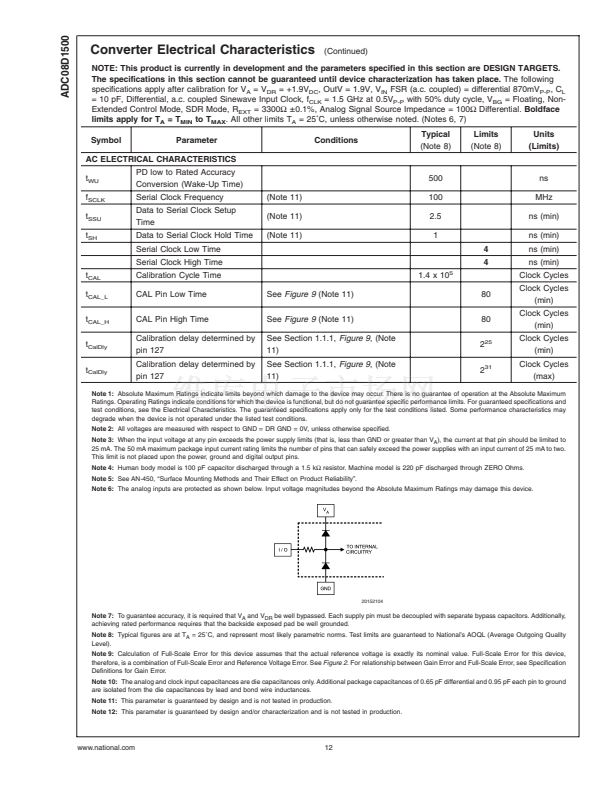
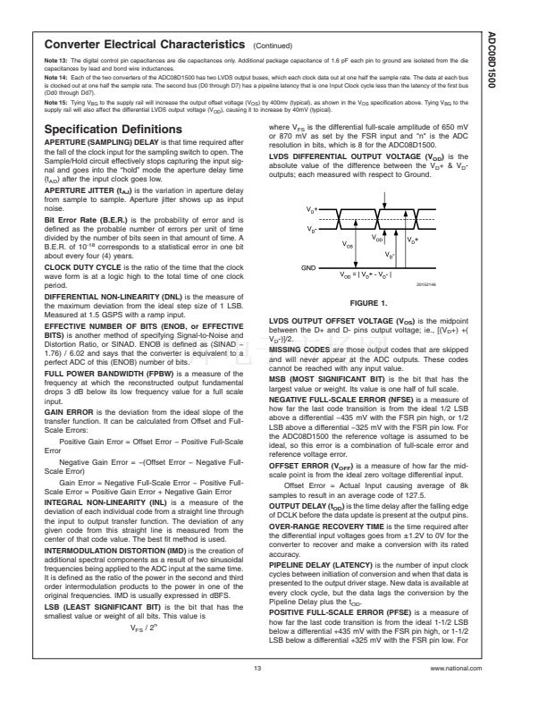
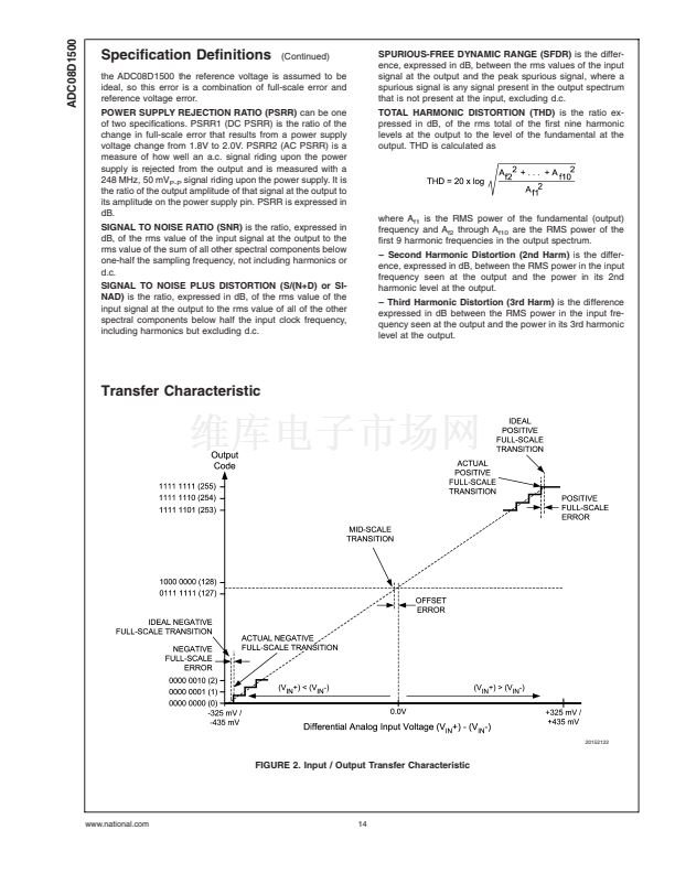
ADC08D1500
1.0 Functional Description
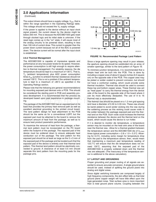
(Continued)
controls are disabled. These pins are OutV (pin 3), OutEdge/
DDR (pin 4), FSR (pin 14) and CalDly/DES (pin 127). See
Section 1.2 for details on the Extended Control mode.
1.1.4 The Analog Inputs
The ADC08D1500 must be driven with a differential input
signal. Operation with a single-ended signal is not recom-
mended. It is important that the input signals are either a.c.
coupled to the inputs with the V
CMO
pin grounded, or d.c.
coupled with the V
CMO
pin left floating. An input common
mode voltage equal to the V
CMO
output must be provided
when d.c. coupling is used.
Two full-scale range settings are provided with pin 14 (FSR).
A high on pin 14 causes an input full-scale range setting of
870 mV
P-P
, while grounding pin 14 causes an input full-scale
range setting of 650 mV
P-P
. The full-scale range setting
operates equally on both ADCs.
In the Extended Control mode, the full-scale input range can
be set to values between 560 mV
P-P
and 840 mV
P-P
through
a serial interface. See Section 2.2
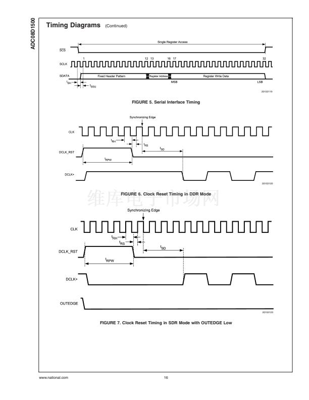
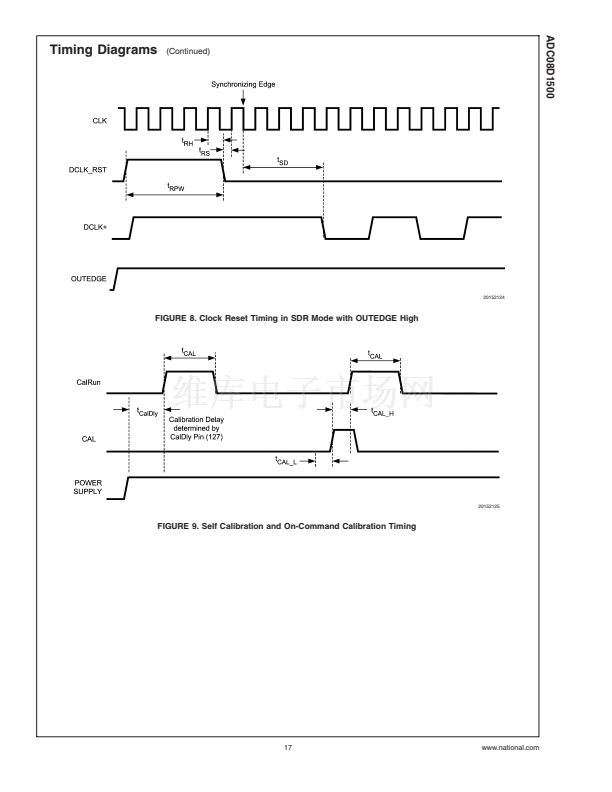
1.1.5 Clocking
The ADC08D1500 must be driven with an a.c. coupled,
differential clock signal. Section 2.3 describes the use of the
clock input pins. A differential LVDS output clock is available
for use in latching the ADC output data into whatever device
is used to receive the data.
The ADC08D1500 offers options for input and output clock-
ing. These options include a choice of Dual Edge Sampling
(DES) or "interleaved mode" where the ADC08D1500 per-
forms as a single device converting at twice the input clock
rate, a choice of which DCLK (DCLK) edge the output data
transitions on, and a choice of Single Data Rate (SDR) or
Double Data Rate (DDR) outputs.
The ADC08D1500 also has the option to use a duty cycle
corrected clock receiver as part of the input clock circuit.
This feature is enabled by default and provides improved
ADC clocking especially in the Dual-Edge Sampling mode
(DES). This circuitry allows the ADC to be clocked with a
signal source having a duty cycle ratio of 80 / 20 % (worst
case) for both the normal and the Dual Edge Sampling
modes.
1.1.5.1 Dual-Edge Sampling
The DES mode allows one of the ADC08D1500鈥檚 inputs (I or
Q Channel) to be sampled by both ADCs. One ADC samples
the input on the positive edge of the input clock and the other
ADC samples the same input on the other edge of the input
clock. A single input is thus sampled twice per input clock
cycle, resulting in an overall sample rate of twice the input
clock frequency, or 3 GSPS with a 1.5 GHz input clock.
In this mode the outputs are interleaved such that the data is
effectively demultiplexed 1:4. Since the sample rate is
doubled, each of the 4 output buses have a 750 MHz output
rate with a 1.5 GHz input clock. All data is available in
parallel. The four bytes of parallel data that are output with
each clock is in the following sampling order, from the earli-
est to the latest: DQd, DId, DQ, DI.
Table 1
indicates what
the outputs represent for the various sampling possibilities.
In the non-extended mode of operation only the "I" input can
be sampled in the DES mode. In the extended mode of
operation the user can select which input is sampled.
The ADC08D1500 also includes an automatic clock phase
background calibration feature which can be used in DES
mode to automatically and continuously adjust the clock
phase of the I and Q channel. This feature removes the need
to adjust the clock phase setting manually and provides
optimal Dual-Edge Sampling ENOB performance.
IMPORTANT NOTE:
The background calibration feature in
DES mode does not replace the requirement for On-
Command Calibration which should be run before entering
DES mode, or if a large swing in ambient temperature is
experienced by the device.
TABLE 1. Input Channel Samples Produced at Data Outputs
Data Outputs (Always
sourced with respect to
fall of DCLK)
DI
DId
DQ
Dual-Edge Sampling Mode (DES)
Normal Sampling Mode
I-Channel Selected
"I" Input Sampled with Fall
of CLK 13 cycles earlier.
"I" Input Sampled with Fall
of CLK 14 cycles earlier.
"Q" Input Sampled with Fall
of CLK 13 cycles earlier.
"I" Input Sampled with Fall
of CLK 13 cycles earlier.
"I" Input Sampled with Fall
of CLK 14 cycles earlier.
"I" Input Sampled with Rise
of CLK 13.5 cycles earlier.
Q-Channel Selected *
"Q" Input Sampled with Fall
of CLK 13 cycles earlier.
"Q" Input Sampled with Fall
of CLK 14 cycles earlier.
"Q" Input Sampled with Rise
of CLK 13.5 cycles earlier.
"Q" Input Sampled with Rise
of CLK 14.5 cycles earlier.
DQd
"Q" Input Sampled with Fall
"I" Input Sampled with Rise
of CLK 14 cycles after being
of CLK 14.5 cycles earlier.
sampled.
* Note that, in the DES mode, the "Q" channel input can only be selected for sampling in the Extended Control Mode.
1.1.5.2 OutEdge Setting
To help ease data capture in the SDR mode, the output data
may be caused to transition on either the positive or the
negative edge of the output data clock (DCLK). This is
chosen with the OutEdge input (pin 4). A high on the Out-
Edge input pin causes the output data to transition on the
rising edge of DCLK, while grounding this input causes the
output to transition on the falling edge of DCLK. See Section
2.4.3.
19
1.1.5.3 Double Data Rate
A choice of single data rate (SDR) or double data rate (DDR)
output is offered. With single data rate the output clock
(DCLK) frequency is the same as the data rate of the two
output buses. With double data rate the DCLK frequency is
half the data rate and data is sent to the outputs on both
edges of DCLK. DDR clocking is enabled in non-Extended
Control mode by allowing pin 4 to float.
www.national.com


 1
1
 2
2
 3
3
 4
4
 5
5
 6
6
 7
7
 8
8
 9
9
 10
10
 11
11
 12
12
 13
13
 14
14
 15
15
 16
16
 17
17
 18
18
 19
19
 20
20
 21
21
 22
22
 23
23
 24
24
 25
25
 26
26
 27
27
 28
28
 29
29
 30
30
 31
31
 32
32
 33
33
