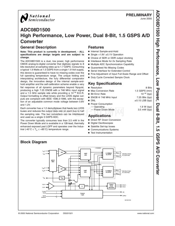
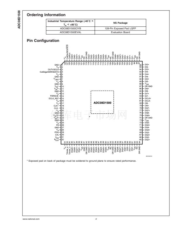
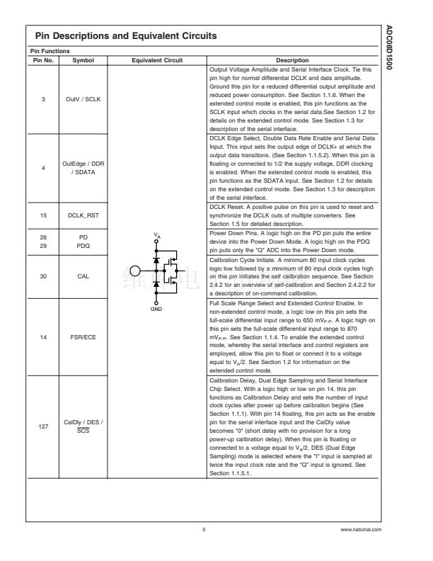
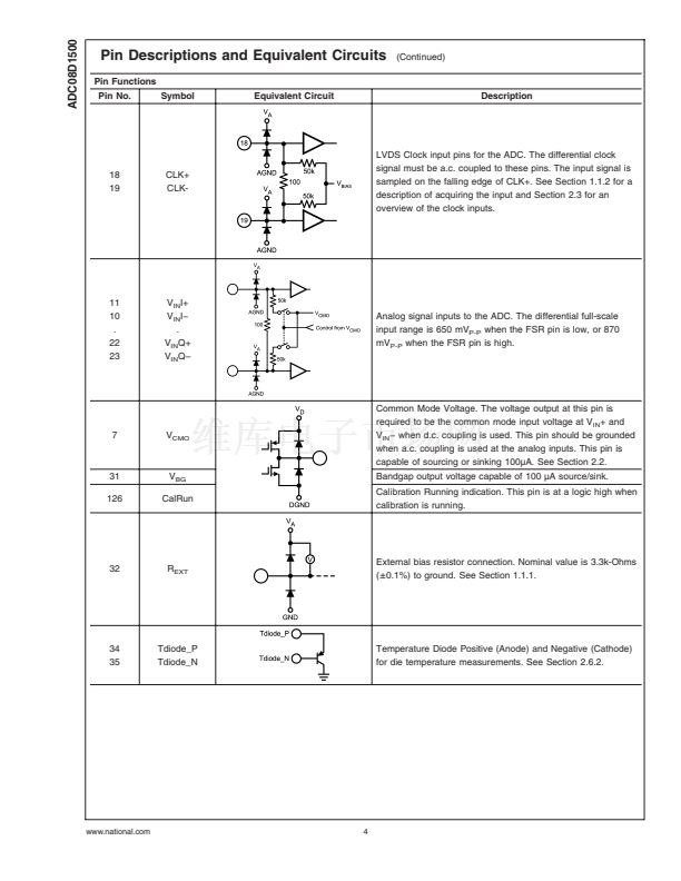
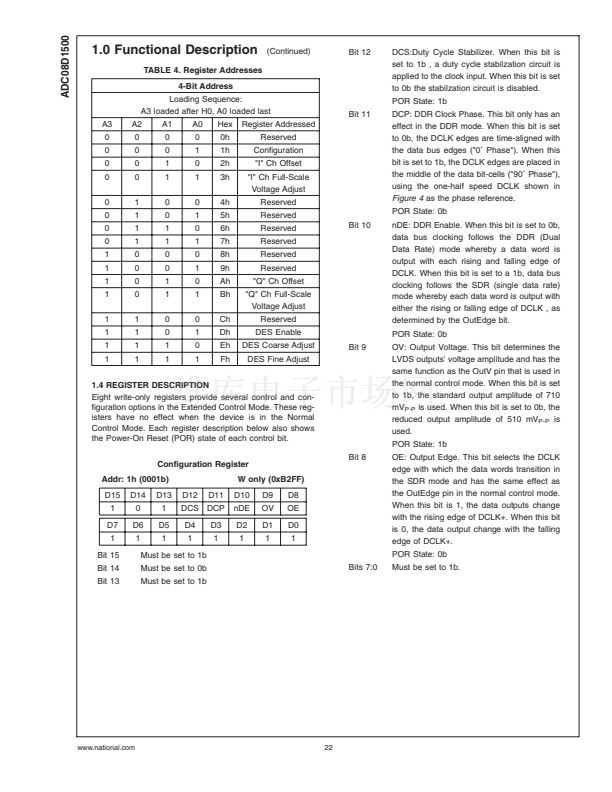
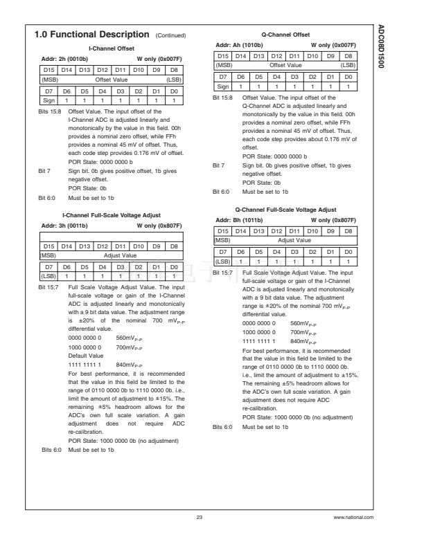
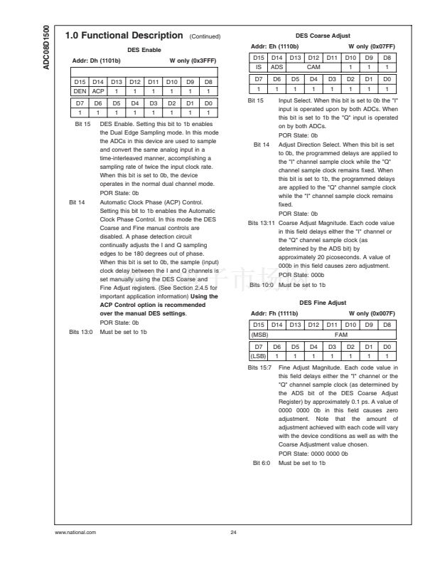
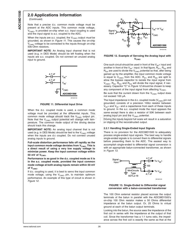
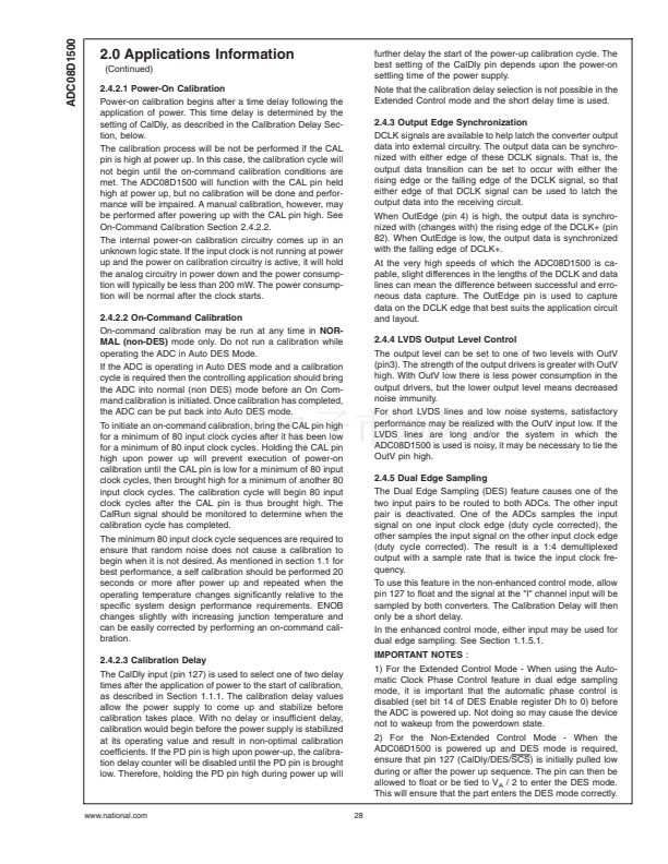
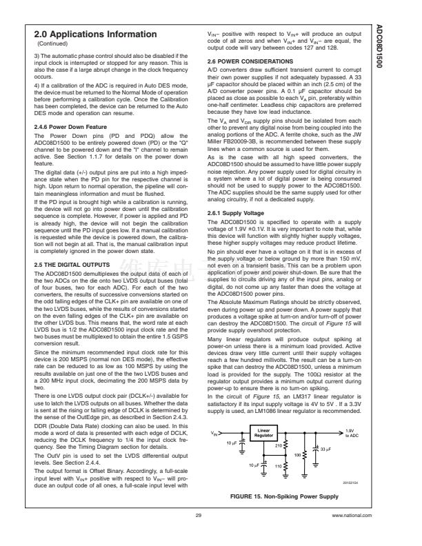
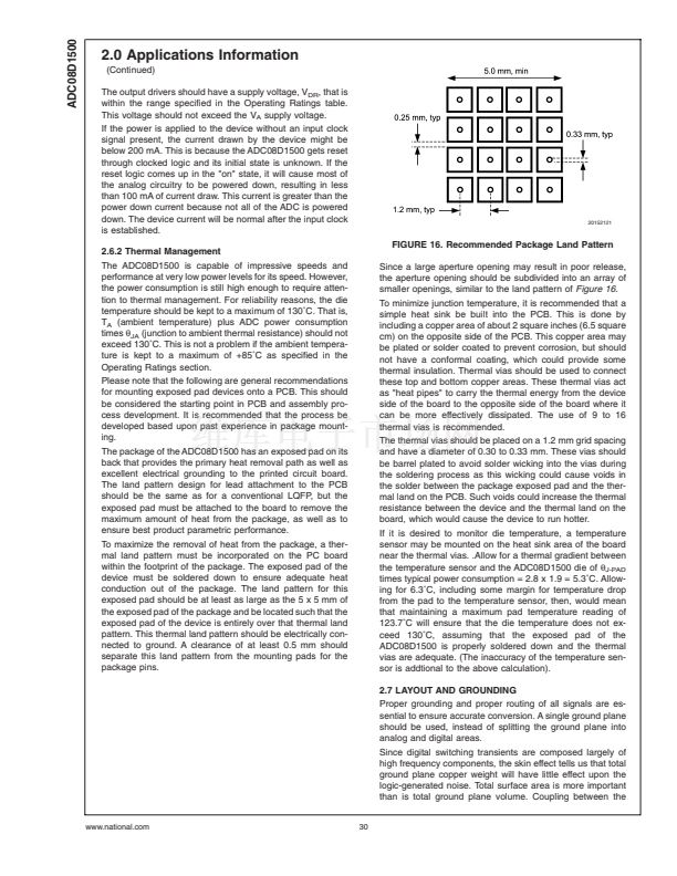
ADC08D1500
2.0 Applications Information
(Continued)
Driving the V
BG
pin to change the reference voltage.
As
mentioned in Section 2.1, the reference voltage is intended
to be fixed to provide one of two different full-scale values
(650 mV
P-P
and 870 mV
P-P
). Over driving this pin will not
change the full scale value, but can be used to change the
LVDS common mode voltage from 0.8V to 1.2V by tying the
V
BG
pin to V
A
.
Driving the clock input with an excessively high level
signal.
The ADC input clock level should not exceed the
level described in the Operating Ratings Table or the input
offset could change.
Inadequate input clock levels.
As described in Section 2.3,
insufficient input clock levels can result in poor performance.
Excessive input clock levels could result in the introduction
of an input offset.
Using a clock source with excessive jitter, using an
excessively long input clock signal trace, or having
other signals coupled to the input clock signal trace.
This will cause the sampling interval to vary, causing exces-
sive output noise and a reduction in SNR performance.
Failure to provide adequate heat removal.
As described in
Section 2.6.2, it is important to provide adequate heat re-
moval to ensure device reliability. This can either be done
with adequate air flow or the use of a simple heat sink built
into the board. The backside pad should be grounded for
best performance.
www.national.com
32


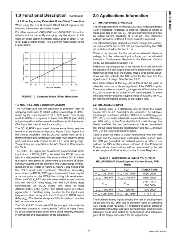
 1
1
 2
2
 3
3
 4
4
 5
5
 6
6
 7
7
 8
8
 9
9
 10
10
 11
11
 12
12
 13
13
 14
14
 15
15
 16
16
 17
17
 18
18
 19
19
 20
20
 21
21
 22
22
 23
23
 24
24
 25
25
 26
26
 27
27
 28
28
 29
29
 30
30
 31
31
 32
32
 33
33
