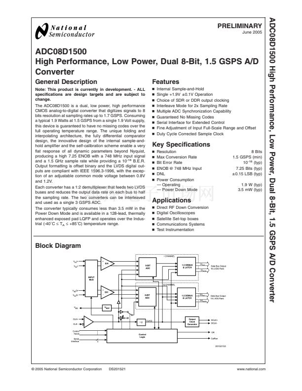
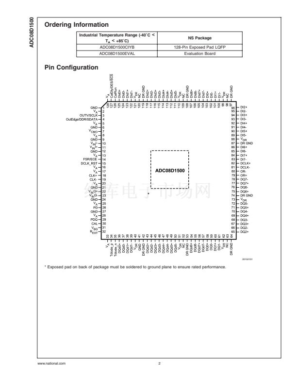
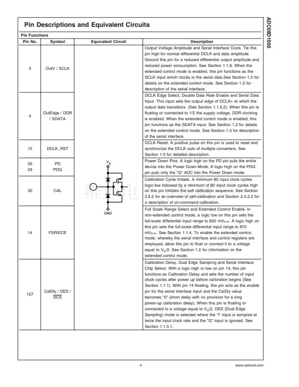
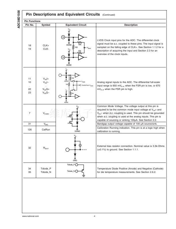
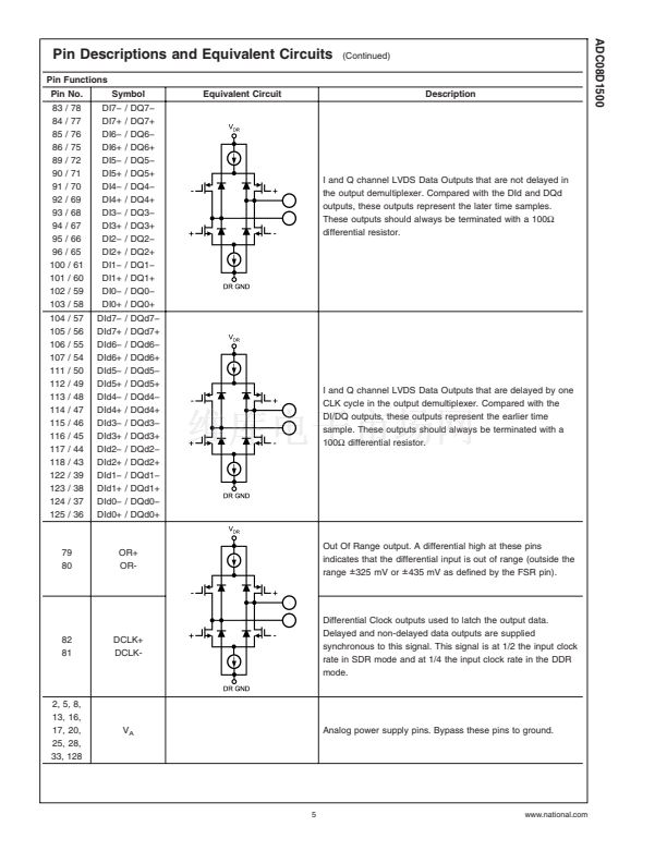
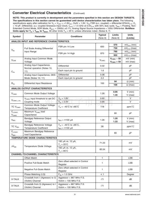
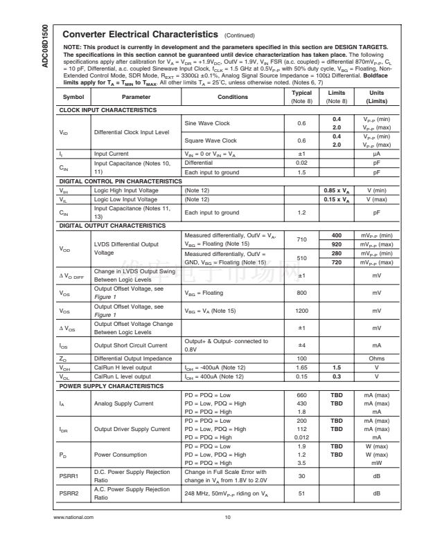
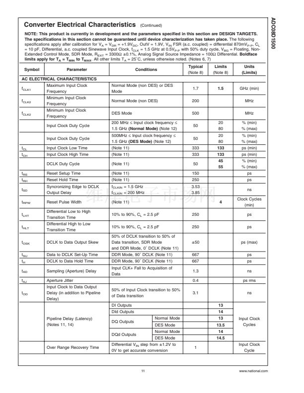
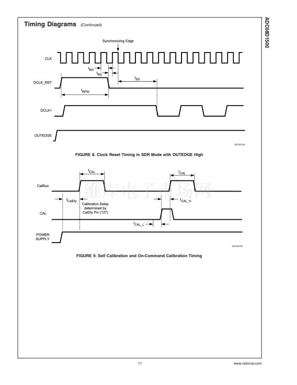
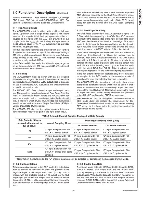
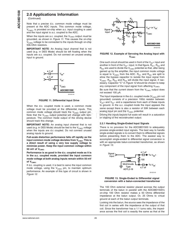
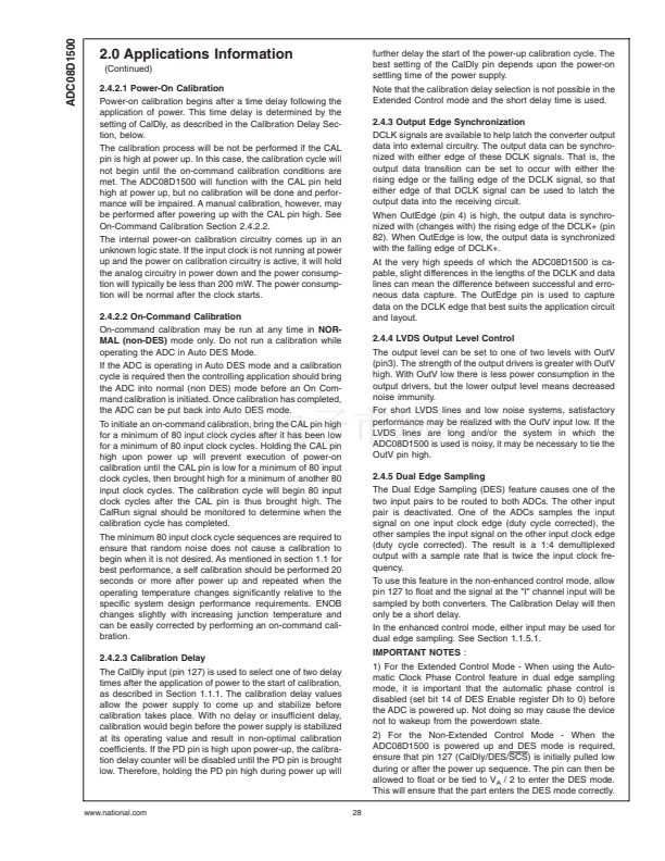
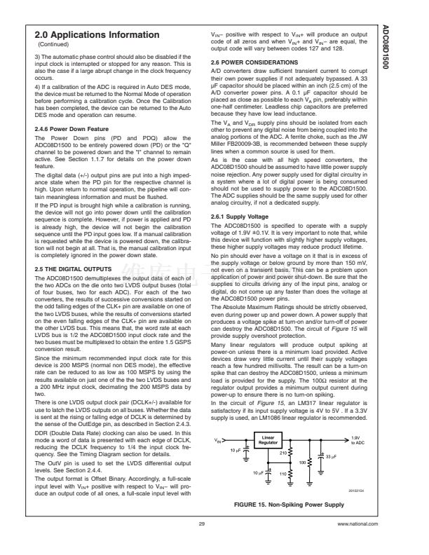
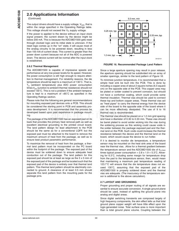
ADC08D1500
1.0 Functional Description
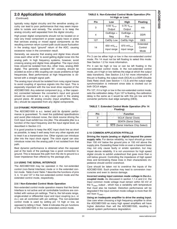
1.1.6 The LVDS Outputs
(Continued)
The data outputs, the Out Of Range (OR) and DCLK, are
LVDS. Output current sources provide 3 mA of output current
to a differential 100 Ohm load when the OutV input (pin 14)
is high or 2.2 mA when the OutV input is low. For short LVDS
lines and low noise systems, satisfactory performance may
be realized with the OutV input low, which results in lower
power consumption. If the LVDS lines are long and/or the
system in which the ADC08D1500 is used is noisy, it may be
necessary to tie the OutV pin high.
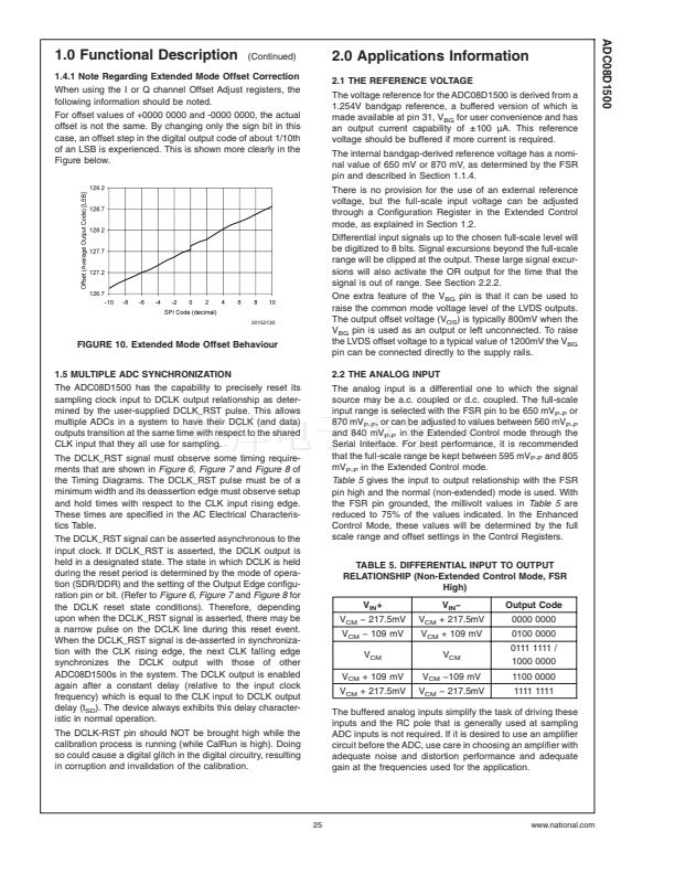
The LVDS data output have a typical common mode voltage
of 800mV when the V
BG
pin is unconnected and floating.
This common mode voltage can be increased to 1.2V by
tying the V
BG
pin to V
A
if a higher common mode is required.
1.1.7 Power Down
The ADC08D1500 is in the active state when the Power
Down pin (PD) is low. When the PD pin is high, the device is
in the power down mode. In this power down mode the data
output pins (positive and negative) are put into a high imped-
ance state and the devices power consumption is reduced to
a minimal level. The DCLK+/- and OR +/- are not tri-stated,
they are weakly pulled down to ground internally. Therefore
when both I and Q are powered down the DCLK +/- and OR
+/- should not be terminated to a DC voltage.
A high on the PDQ pin will power down the "Q" channel and
leave the "I" channel active. There is no provision to power
down the "I" channel independently of the "Q" channel. Upon
return to normal operation, the pipeline will contain meaning-
less information.
If the PD input is brought high while a calibration is running,
the device will not go into power down until the calibration
sequence is complete. However, if power is applied and PD
is already high, the device will not begin the calibration
sequence until the PD input goes low. If a manual calibration
is requested while the device is powered down, the calibra-
tion will not begin at all. That is, the manual calibration input
is completely ignored in the power down state. Calibration
will function with the "Q" channel powered down, but that
channel will not be calibrated if PDQ is high. If the "Q"
channel is subsequently to be used, it is necessary to per-
form a calibration after PDQ is brought low.
1.2 NORMAL/EXTENDED CONTROL
The ADC08D1500 may be operated in one of two modes. In
the simpler standard control mode, the user affects available
configuration and control of the device through several con-
trol pins. The "extended control mode" provides additional
configuration and control options through a serial interface
and a set of 8 registers. The two control modes are selected
with pin 14 (FSR/ECE: Extended Control Enable). The
choice of control modes is required to be a fixed selection
and is not intended to be switched dynamically while the
device is operational.
Table 2
shows how several of the device features are af-
fected by the control mode chosen.
TABLE 2. Features and modes
Feature
SDR or DDR Clocking
Normal Control Mode
Selected with pin 4
Extended Control Mode
Selected with DE bit in the
Configuration Register
Selected with DCP bit in the
Configuration Register. See
Section
1.4 REGISTER DESCRIPTION
Selected with the OE bit in the
Configuration Register
Selected with the OV bit (9)in the
Configuration Register
Short delay only.
Up to 512 step adjustments over a
nominal range of 560 mV to 840 mV.
Separate range selected for I- and
Q-Channels. Selected using registers
3H and Bh
Separate
卤
45 mV adjustments in 512
steps for each channel using registers
2h and Ah
Enabled through DES Enable Register
Either I- or Q-Channel input may be
sampled by both ADCs
Automatic Clock Phase control can be
selected by setting bit 14 in the DES
Enable register (Dh). The clock phase
can also be adjusted manually through
the Coarse & Fine registers (Eh and
Fh)
DDR Clock Phase
SDR Data transitions with rising or
falling DCLK edge
LVDS output level
Power-On Calibration Delay
Not Selectable (0藲 Phase Only)
Selected with pin 4
Selected with pin 3
Delay Selected with pin 127
Options (650 mV
P-P
or 870 mV
P-P
)
selected with pin 14. Selected range
applies to both channels.
Full-Scale Range
Input Offset Adjust
Dual Edge Sampling Selection
Dual Edge Sampling Input Channel
Selection
Not possible
Enabled with pin 127
Only I-Channel Input can be used
DES Sampling Clock Adjustment
The Clock Phase is adjusted
automatically
www.national.com
20


 1
1
 2
2
 3
3
 4
4
 5
5
 6
6
 7
7
 8
8
 9
9
 10
10
 11
11
 12
12
 13
13
 14
14
 15
15
 16
16
 17
17
 18
18
 19
19
 20
20
 21
21
 22
22
 23
23
 24
24
 25
25
 26
26
 27
27
 28
28
 29
29
 30
30
 31
31
 32
32
 33
33
