ADC08D1500
1.0 Functional Description
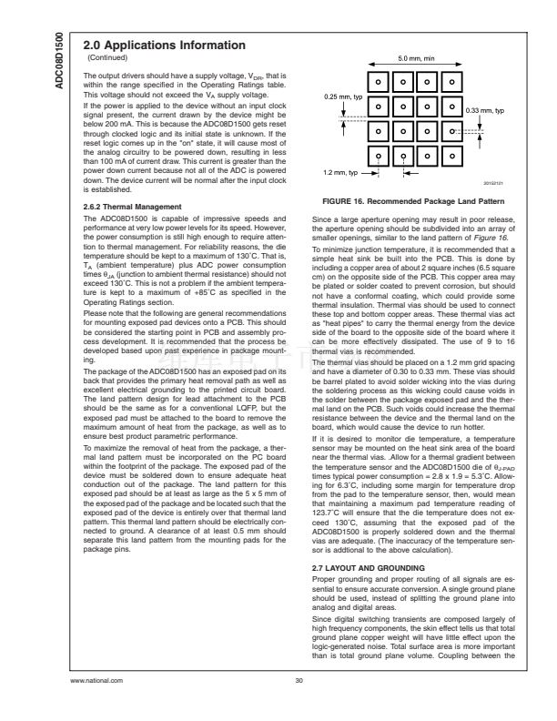
(Continued)
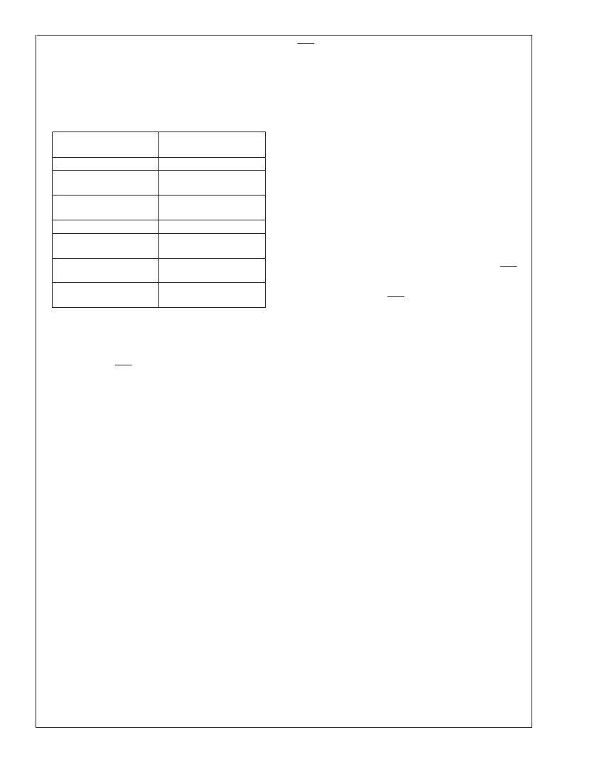
The default state of the Extended Control Mode is set upon
power-on reset (internally performed by the device) and is
shown in
Table 3.
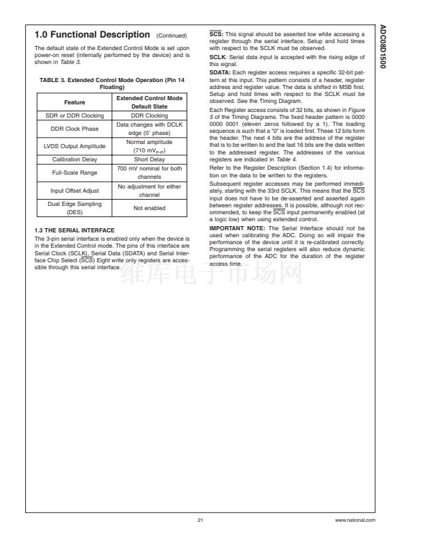
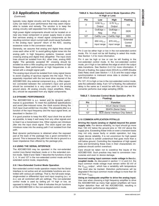
TABLE 3. Extended Control Mode Operation (Pin 14
Floating)
Feature
SDR or DDR Clocking
DDR Clock Phase
LVDS Output Amplitude
Calibration Delay
Full-Scale Range
Input Offset Adjust
Dual Edge Sampling
(DES)
Extended Control Mode
Default State
DDR Clocking
Data changes with DCLK
edge (0藲 phase)
Normal amplitude
(710 mV
P-P
)
Short Delay
700 mV nominal for both
channels
No adjustment for either
channel
Not enabled
SCS:
This signal should be asserted low while accessing a
register through the serial interface. Setup and hold times
with respect to the SCLK must be observed.
SCLK:
Serial data input is accepted with the rising edge of
this signal.
SDATA:
Each register access requires a specific 32-bit pat-
tern at this input. This pattern consists of a header, register
address and register value. The data is shifted in MSB first.
Setup and hold times with respect to the SCLK must be
observed. See the Timing Diagram.
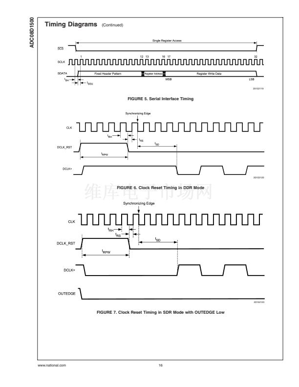
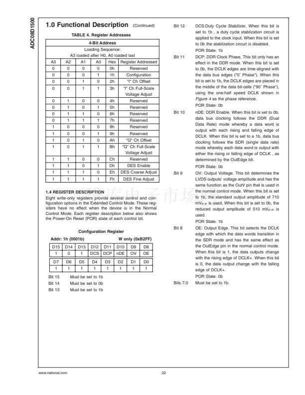
Each Register access consists of 32 bits, as shown in
Figure
5
of the Timing Diagrams. The fixed header pattern is 0000
0000 0001 (eleven zeros followed by a 1). The loading
sequence is such that a "0" is loaded first. These 12 bits form
the header. The next 4 bits are the address of the register
that is to be written to and the last 16 bits are the data written
to the addressed register. The addresses of the various
registers are indicated in
Table 4.
Refer to the Register Description (Section 1.4) for informa-
tion on the data to be written to the registers.
Subsequent register accesses may be performed immedi-
ately, starting with the 33rd SCLK. This means that the SCS
input does not have to be de-asserted and asserted again
between register addresses. It is possible, although not rec-
ommended, to keep the SCS input permanently enabled (at
a logic low) when using extended control.
IMPORTANT NOTE:
The Serial Interface should not be
used when calibrating the ADC. Doing so will impair the
performance of the device until it is re-calibrated correctly.
Programming the serial registers will also reduce dynamic
performance of the ADC for the duration of the register
access time.
1.3 THE SERIAL INTERFACE
The 3-pin serial interface is enabled only when the device is
in the Extended Control mode. The pins of this interface are
Serial Clock (SCLK), Serial Data (SDATA) and Serial Inter-
face Chip Select (SCS) Eight write only registers are acces-
sible through this serial interface.
21
www.national.com


 1
1
 2
2
 3
3
 4
4
 5
5
 6
6
 7
7
 8
8
 9
9
 10
10
 11
11
 12
12
 13
13
 14
14
 15
15
 16
16
 17
17
 18
18
 19
19
 20
20
 21
21
 22
22
 23
23
 24
24
 25
25
 26
26
 27
27
 28
28
 29
29
 30
30
 31
31
 32
32
 33
33
