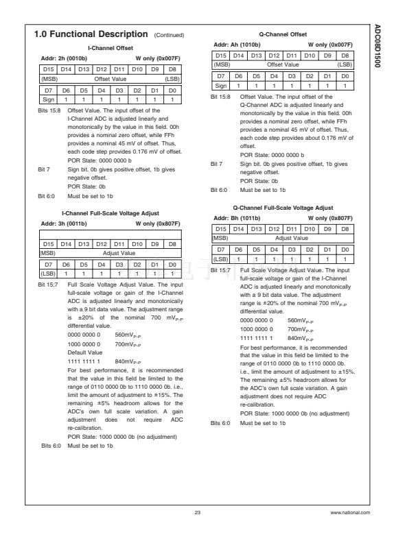
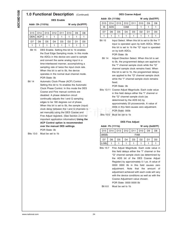
ADC08D1500
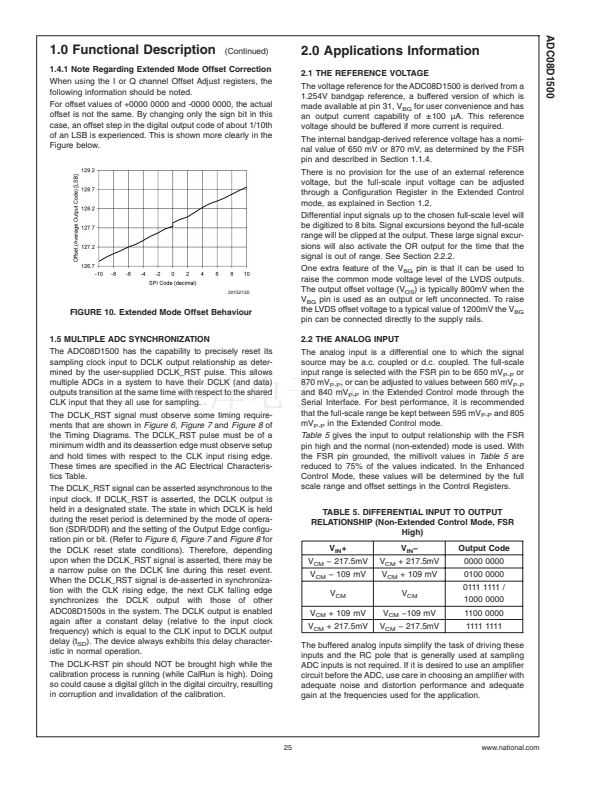
1.0 Functional Description
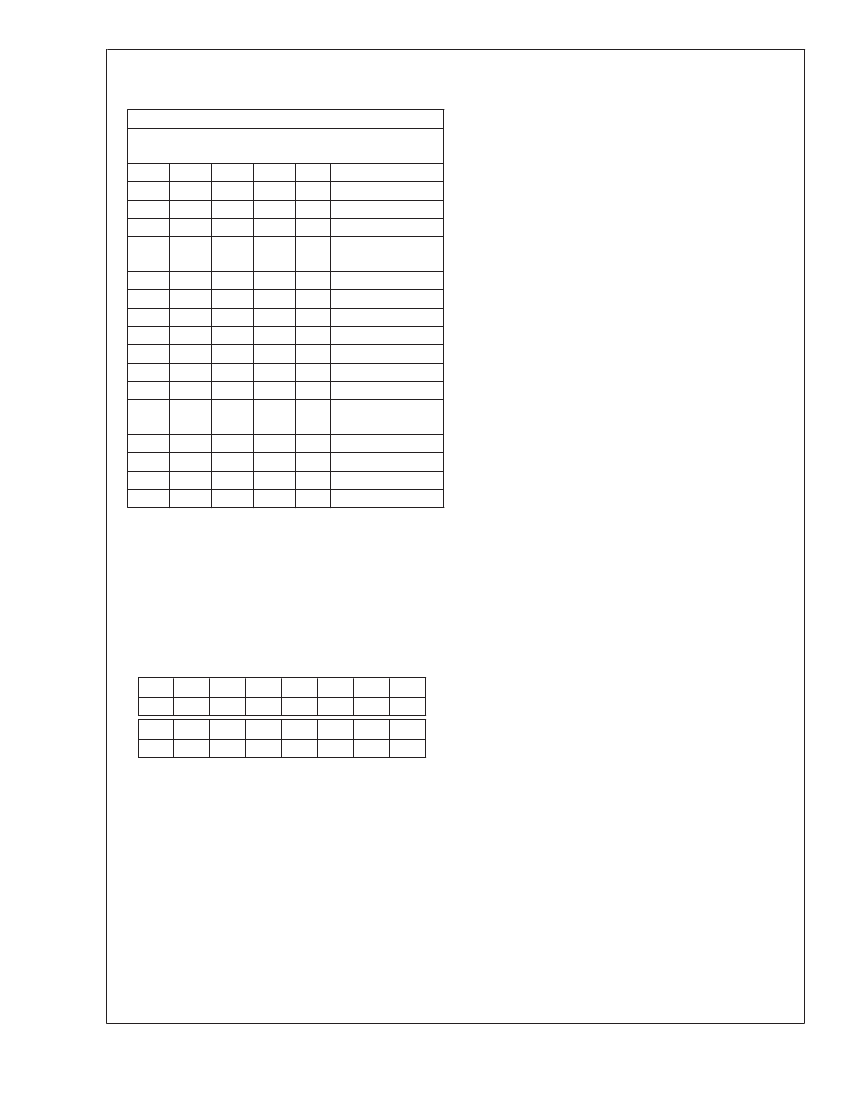
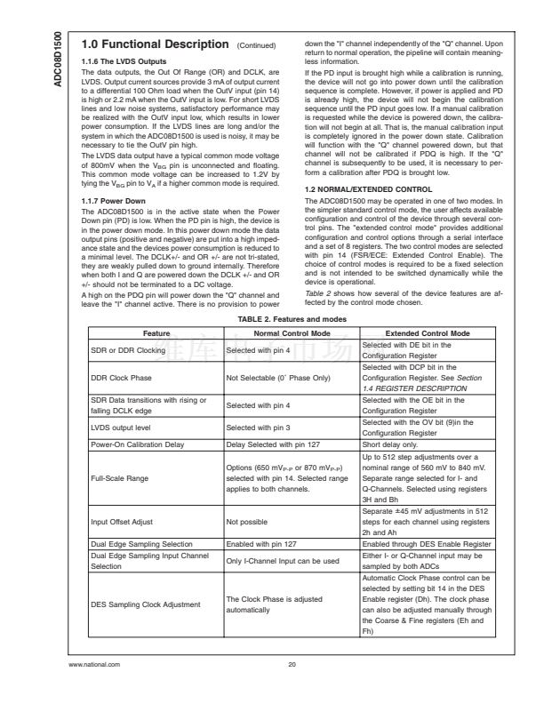
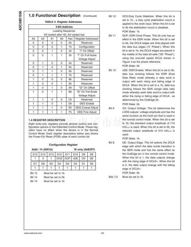
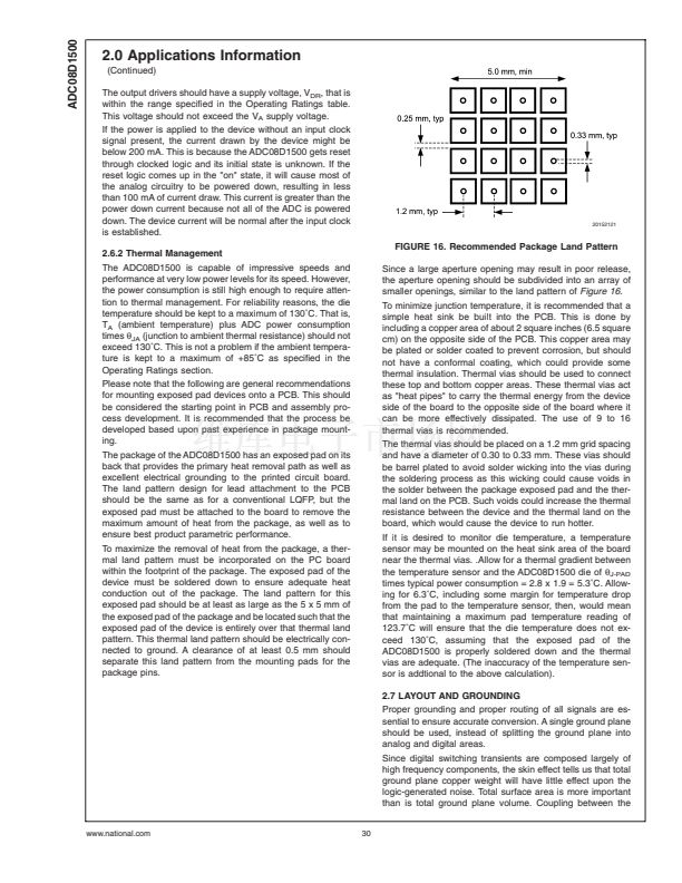
TABLE 4. Register Addresses
4-Bit Address
(Continued)
Bit 12
DCS:Duty Cycle Stabilizer. When this bit is
set to 1b , a duty cycle stabilzation circuit is
applied to the clock input. When this bit is set
to 0b the stabilzation circuit is disabled.
POR State: 1b
DCP: DDR Clock Phase. This bit only has an
effect in the DDR mode. When this bit is set
to 0b, the DCLK edges are time-aligned with
the data bus edges ("0藲 Phase"). When this
bit is set to 1b, the DCLK edges are placed in
the middle of the data bit-cells ("90藲 Phase"),
using the one-half speed DCLK shown in
Figure 4
as the phase reference.
POR State: 0b
nDE: DDR Enable. When this bit is set to 0b,
data bus clocking follows the DDR (Dual
Data Rate) mode whereby a data word is
output with each rising and falling edge of
DCLK. When this bit is set to a 1b, data bus
clocking follows the SDR (single data rate)
mode whereby each data word is output with
either the rising or falling edge of DCLK , as
determined by the OutEdge bit.
POR State: 0b
OV: Output Voltage. This bit determines the
LVDS outputs鈥?voltage amplitude and has the
same function as the OutV pin that is used in
the normal control mode. When this bit is set
to 1b, the standard output amplitude of 710
mV
P-P
is used. When this bit is set to 0b, the
reduced output amplitude of 510 mV
P-P
is
used.
POR State: 1b
OE: Output Edge. This bit selects the DCLK
edge with which the data words transition in
the SDR mode and has the same effect as
the OutEdge pin in the normal control mode.
When this bit is 1, the data outputs change
with the rising edge of DCLK+. When this bit
is 0, the data output change with the falling
edge of DCLK+.
POR State: 0b
Must be set to 1b.
Loading Sequence:
A3 loaded after H0, A0 loaded last
A3
0
0
0
0
0
0
0
0
1
1
1
1
1
1
1
1
A2
0
0
0
0
1
1
1
1
0
0
0
0
1
1
1
1
A1
0
0
1
1
0
0
1
1
0
0
1
1
0
0
1
1
A0
0
1
0
1
0
1
0
1
0
1
0
1
0
1
0
1
Hex
0h
1h
2h
3h
4h
5h
6h
7h
8h
9h
Ah
Bh
Ch
Dh
Eh
Fh
Register Addressed
Reserved
Configuration
"I" Ch Offset
"I" Ch Full-Scale
Voltage Adjust
Reserved
Reserved
Reserved
Reserved
Reserved
Reserved
"Q" Ch Offset
"Q" Ch Full-Scale
Voltage Adjust
Reserved
DES Enable
DES Coarse Adjust
DES Fine Adjust
Bit 11
Bit 10
Bit 9
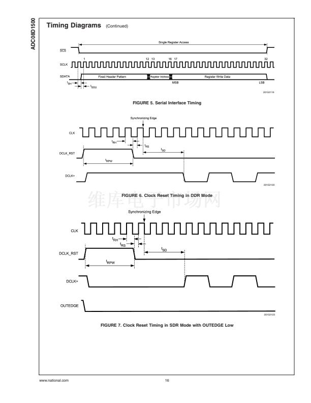
1.4 REGISTER DESCRIPTION
Eight write-only registers provide several control and con-
figuration options in the Extended Control Mode. These reg-
isters have no effect when the device is in the Normal
Control Mode. Each register description below also shows
the Power-On Reset (POR) state of each control bit.
Configuration Register
Addr: 1h (0001b)
D15
1
D7
1
Bit 15
Bit 14
Bit 13
D14
0
D6
1
D13
1
D5
1
D12
D11
W only (0xB2FF)
D10
nDE
D2
1
D9
OV
D1
1
D8
OE
D0
1
Bit 8
DCS DCP
D4
1
D3
1
Must be set to 1b
Must be set to 0b
Must be set to 1b
Bits 7:0
www.national.com
22


 1
1
 2
2
 3
3
 4
4
 5
5
 6
6
 7
7
 8
8
 9
9
 10
10
 11
11
 12
12
 13
13
 14
14
 15
15
 16
16
 17
17
 18
18
 19
19
 20
20
 21
21
 22
22
 23
23
 24
24
 25
25
 26
26
 27
27
 28
28
 29
29
 30
30
 31
31
 32
32
 33
33
