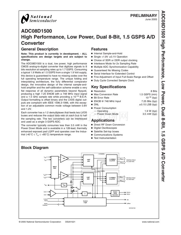
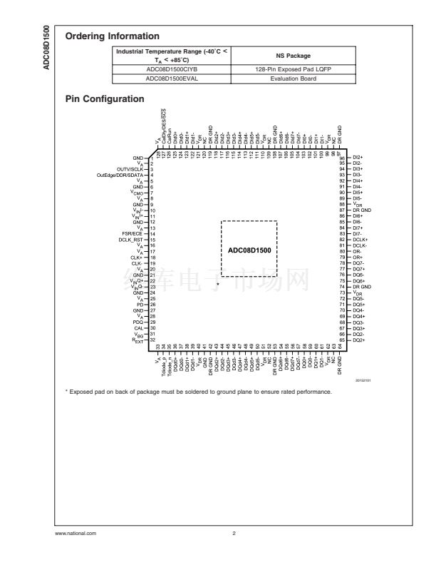
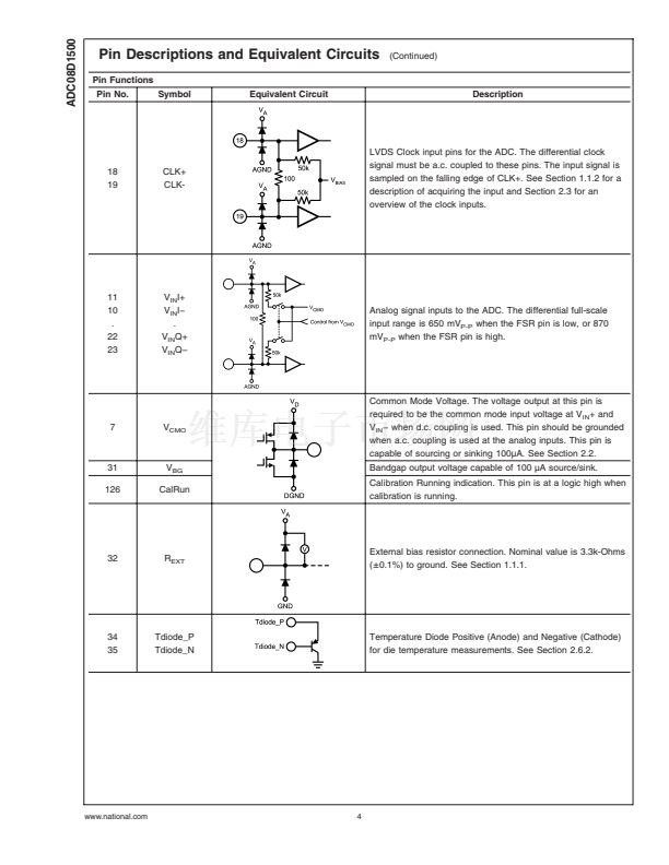
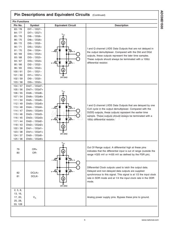
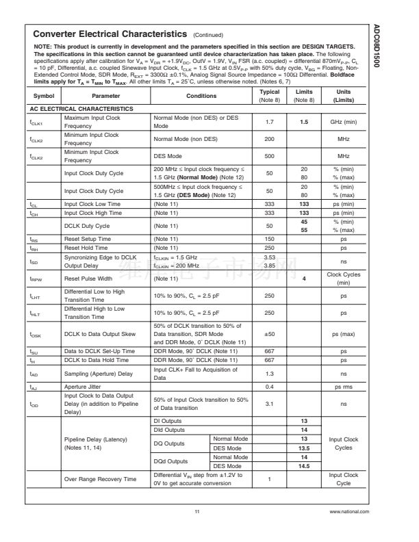
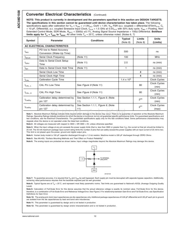
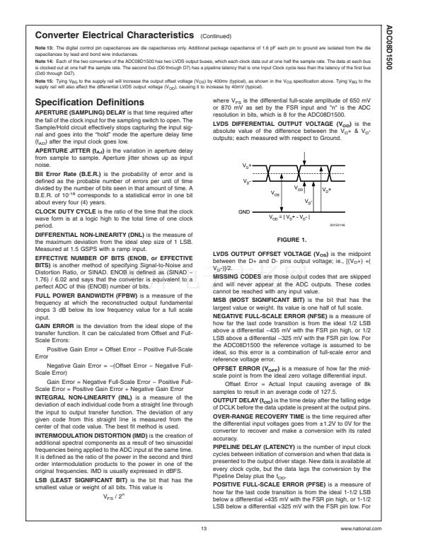
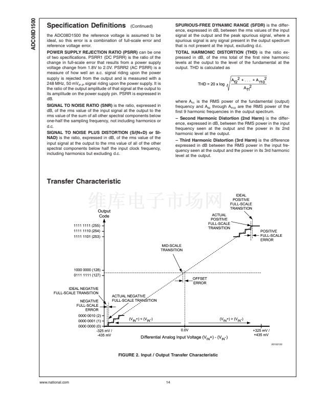
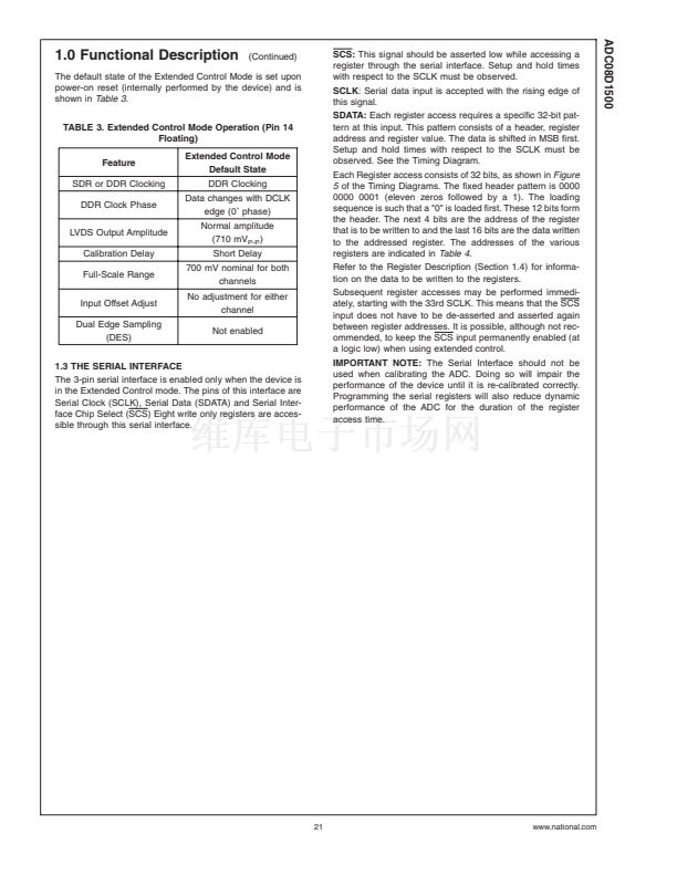
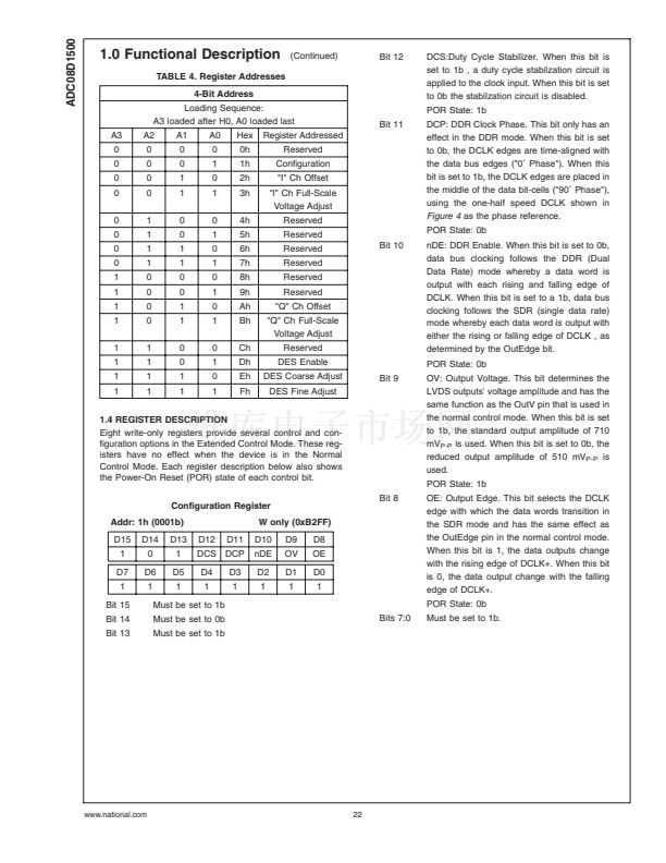
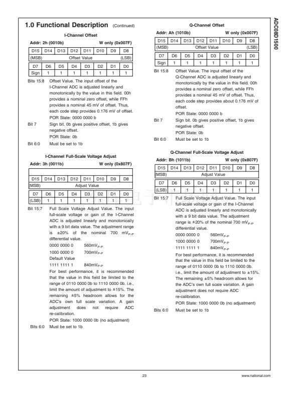
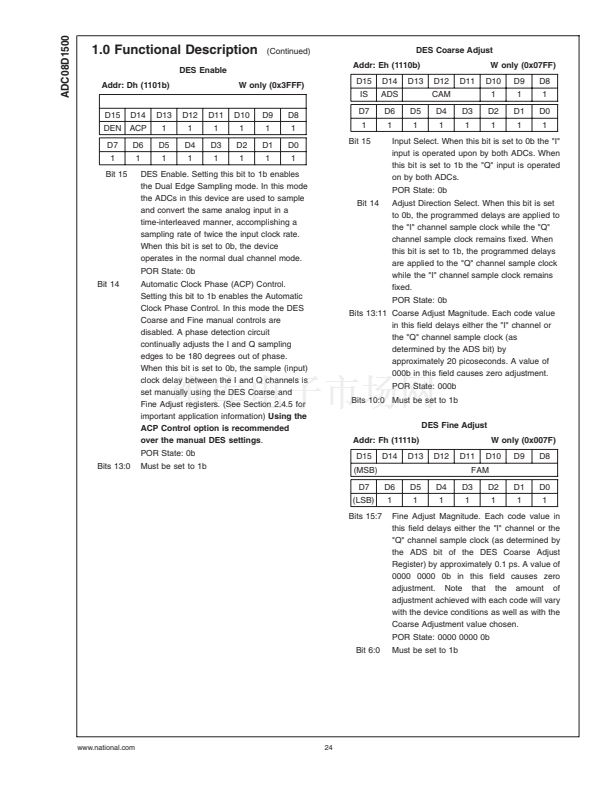
ADC08D1500
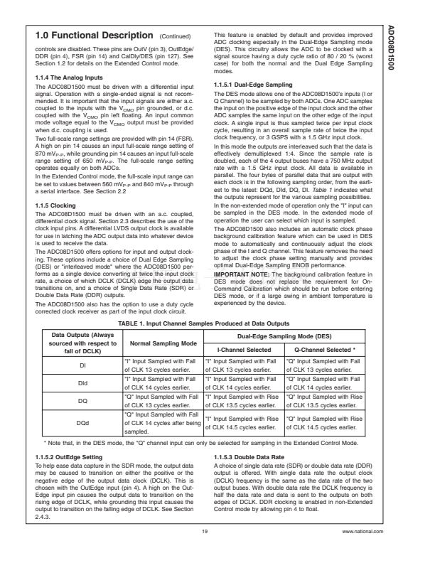
1.0 Functional Description
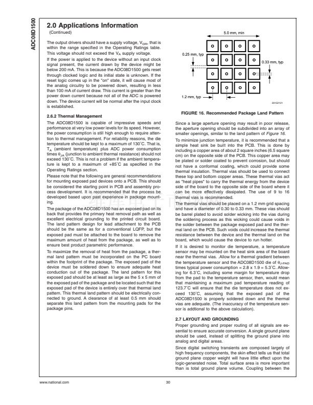
(Continued)
2.0 Applications Information
2.1 THE REFERENCE VOLTAGE
The voltage reference for the ADC08D1500 is derived from a
1.254V bandgap reference, a buffered version of which is
made available at pin 31, V
BG
for user convenience and has
an output current capability of
卤
100 碌A. This reference
voltage should be buffered if more current is required.
The internal bandgap-derived reference voltage has a nomi-
nal value of 650 mV or 870 mV, as determined by the FSR
pin and described in Section 1.1.4.
There is no provision for the use of an external reference
voltage, but the full-scale input voltage can be adjusted
through a Configuration Register in the Extended Control
mode, as explained in Section 1.2.
Differential input signals up to the chosen full-scale level will
be digitized to 8 bits. Signal excursions beyond the full-scale
range will be clipped at the output. These large signal excur-
sions will also activate the OR output for the time that the
signal is out of range. See Section 2.2.2.
One extra feature of the V
BG
pin is that it can be used to
raise the common mode voltage level of the LVDS outputs.
The output offset voltage (V
OS
) is typically 800mV when the
V
BG
pin is used as an output or left unconnected. To raise
the LVDS offset voltage to a typical value of 1200mV the V
BG
pin can be connected directly to the supply rails.
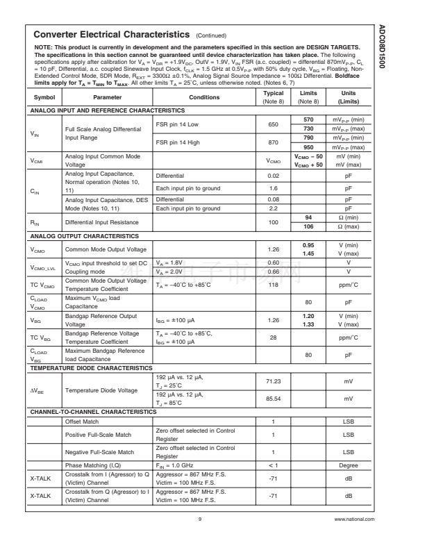
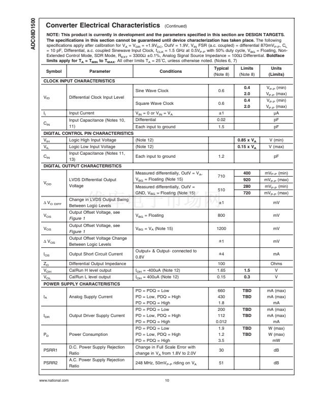
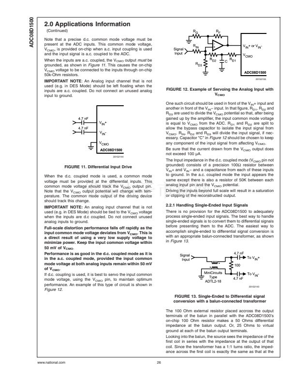
2.2 THE ANALOG INPUT
The analog input is a differential one to which the signal
source may be a.c. coupled or d.c. coupled. The full-scale
input range is selected with the FSR pin to be 650 mV
P-P
or
870 mV
P-P
, or can be adjusted to values between 560 mV
P-P
and 840 mV
P-P
in the Extended Control mode through the
Serial Interface. For best performance, it is recommended
that the full-scale range be kept between 595 mV
P-P
and 805
mV
P-P
in the Extended Control mode.
Table 5
gives the input to output relationship with the FSR
pin high and the normal (non-extended) mode is used. With
the FSR pin grounded, the millivolt values in
Table 5
are
reduced to 75% of the values indicated. In the Enhanced
Control Mode, these values will be determined by the full
scale range and offset settings in the Control Registers.
TABLE 5. DIFFERENTIAL INPUT TO OUTPUT
RELATIONSHIP (Non-Extended Control Mode, FSR
High)
V
IN
+
V
CM
鈭?217.5mV
V
CM
鈭?109 mV
V
CM
V
CM
+ 109 mV
V
CM
+ 217.5mV
V
IN
鈭?/div>
V
CM
+ 217.5mV
V
CM
+ 109 mV
V
CM
V
CM
鈭?09 mV
V
CM
鈭?217.5mV
Output Code
0000 0000
0100 0000
0111 1111 /
1000 0000
1100 0000
1111 1111
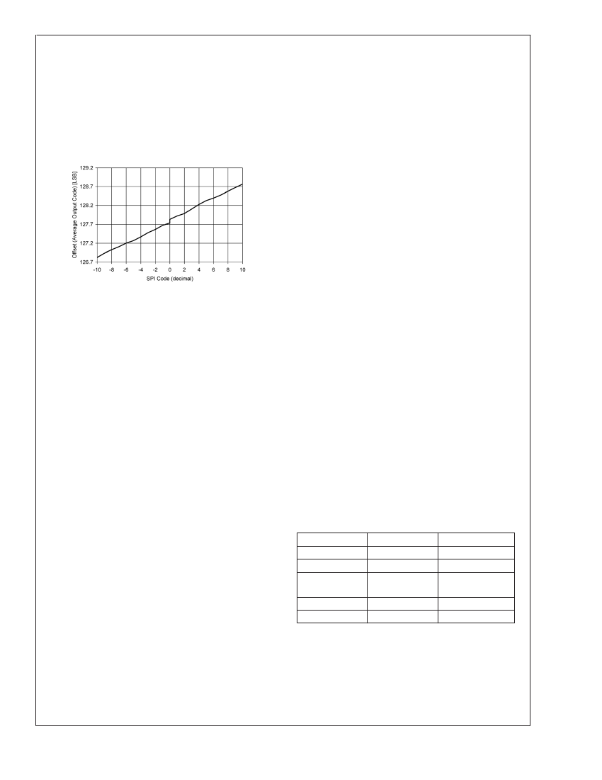
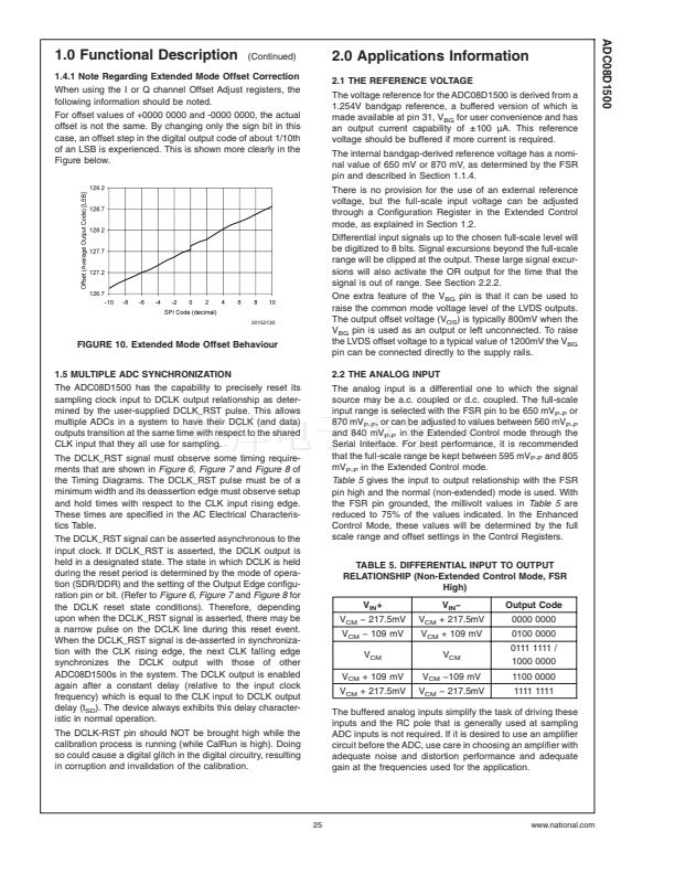
1.4.1 Note Regarding Extended Mode Offset Correction
When using the I or Q channel Offset Adjust registers, the
following information should be noted.
For offset values of +0000 0000 and -0000 0000, the actual
offset is not the same. By changing only the sign bit in this
case, an offset step in the digital output code of about 1/10th
of an LSB is experienced. This is shown more clearly in the
Figure below.
20152130
FIGURE 10. Extended Mode Offset Behaviour
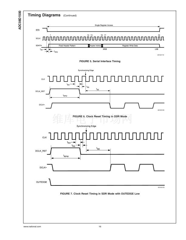
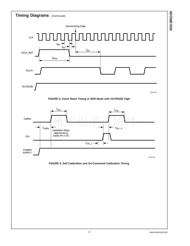
1.5 MULTIPLE ADC SYNCHRONIZATION
The ADC08D1500 has the capability to precisely reset its
sampling clock input to DCLK output relationship as deter-
mined by the user-supplied DCLK_RST pulse. This allows
multiple ADCs in a system to have their DCLK (and data)
outputs transition at the same time with respect to the shared
CLK input that they all use for sampling.
The DCLK_RST signal must observe some timing require-
ments that are shown in
Figure 6, Figure 7
and
Figure 8
of
the Timing Diagrams. The DCLK_RST pulse must be of a
minimum width and its deassertion edge must observe setup
and hold times with respect to the CLK input rising edge.
These times are specified in the AC Electrical Characteris-
tics Table.
The DCLK_RST signal can be asserted asynchronous to the
input clock. If DCLK_RST is asserted, the DCLK output is
held in a designated state. The state in which DCLK is held
during the reset period is determined by the mode of opera-
tion (SDR/DDR) and the setting of the Output Edge configu-
ration pin or bit. (Refer to
Figure 6, Figure 7
and
Figure 8
for
the DCLK reset state conditions). Therefore, depending
upon when the DCLK_RST signal is asserted, there may be
a narrow pulse on the DCLK line during this reset event.
When the DCLK_RST signal is de-asserted in synchroniza-
tion with the CLK rising edge, the next CLK falling edge
synchronizes the DCLK output with those of other
ADC08D1500s in the system. The DCLK output is enabled
again after a constant delay (relative to the input clock
frequency) which is equal to the CLK input to DCLK output
delay (t
SD
). The device always exhibits this delay character-
istic in normal operation.
The DCLK-RST pin should NOT be brought high while the
calibration process is running (while CalRun is high). Doing
so could cause a digital glitch in the digital circuitry, resulting
in corruption and invalidation of the calibration.
The buffered analog inputs simplify the task of driving these
inputs and the RC pole that is generally used at sampling
ADC inputs is not required. If it is desired to use an amplifier
circuit before the ADC, use care in choosing an amplifier with
adequate noise and distortion performance and adequate
gain at the frequencies used for the application.
25
www.national.com


 1
1
 2
2
 3
3
 4
4
 5
5
 6
6
 7
7
 8
8
 9
9
 10
10
 11
11
 12
12
 13
13
 14
14
 15
15
 16
16
 17
17
 18
18
 19
19
 20
20
 21
21
 22
22
 23
23
 24
24
 25
25
 26
26
 27
27
 28
28
 29
29
 30
30
 31
31
 32
32
 33
33
