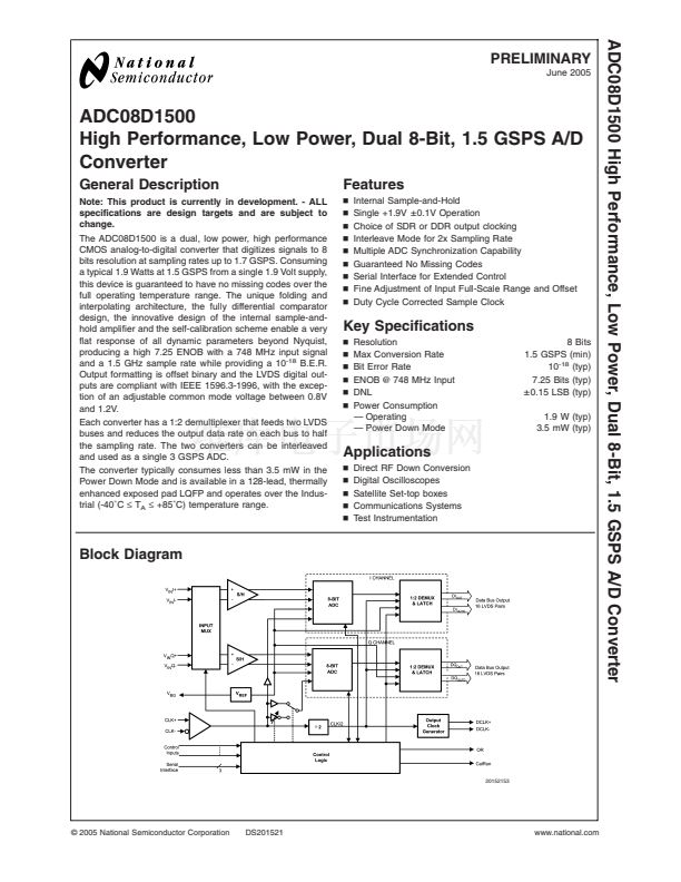
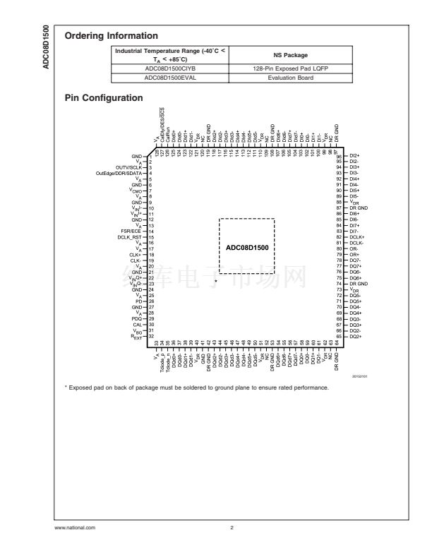
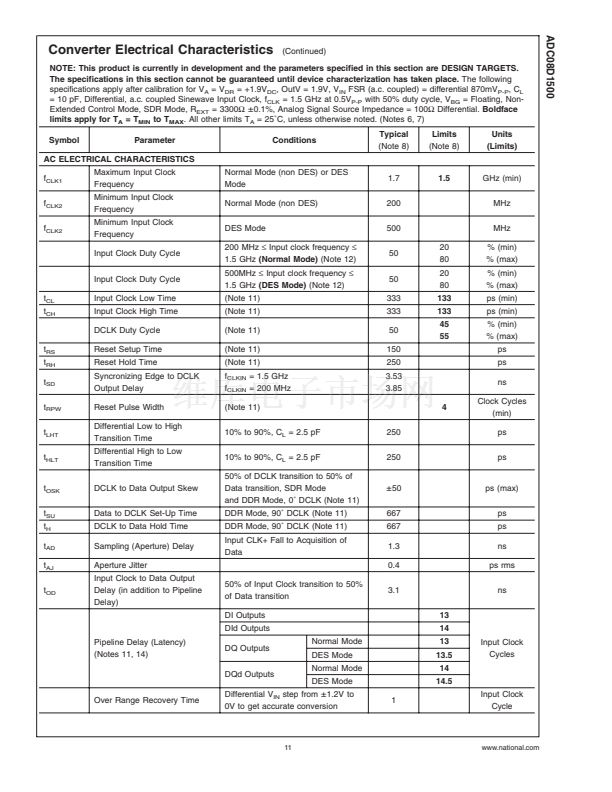
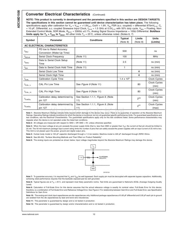
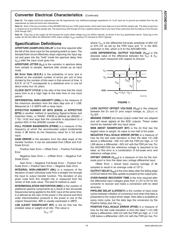
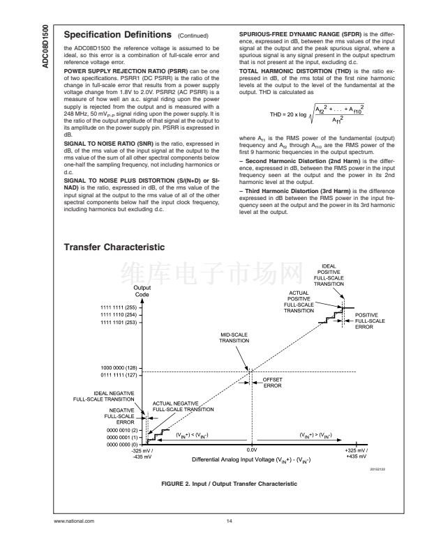
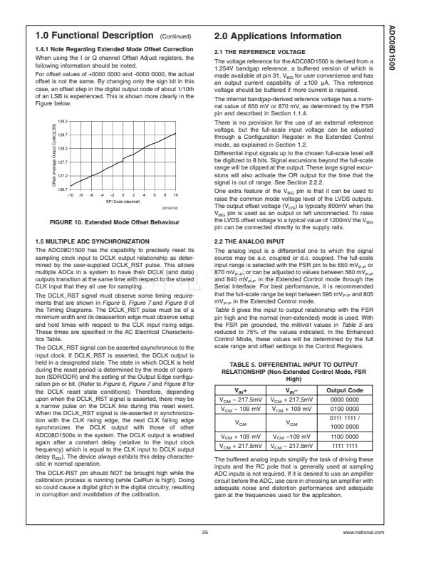
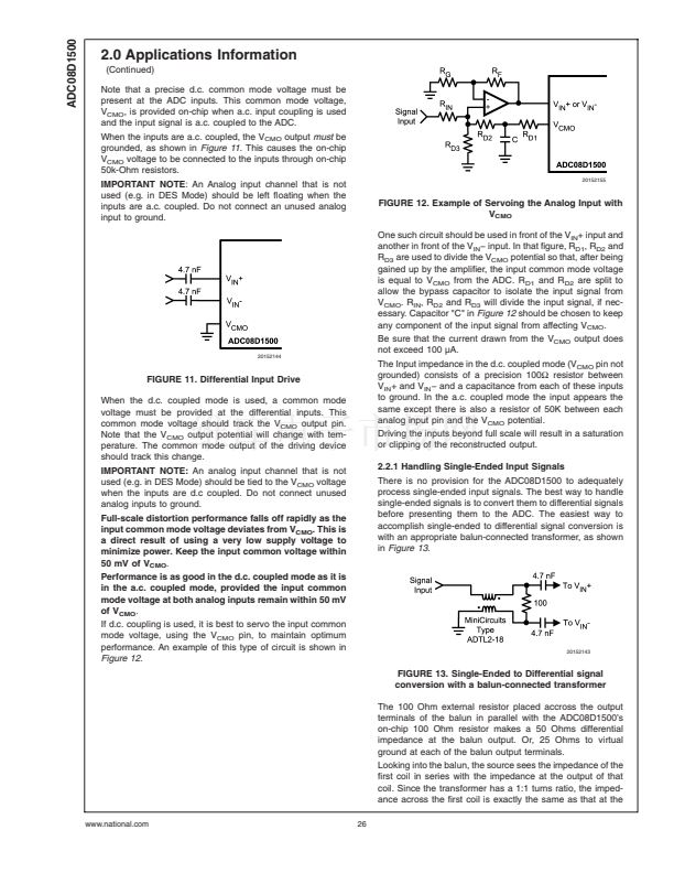
ADC08D1500
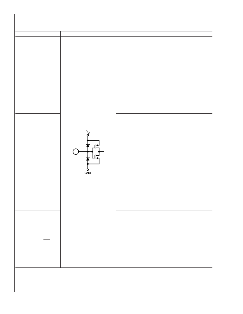
Pin Descriptions and Equivalent Circuits
Pin Functions
Pin No.
Symbol
Equivalent Circuit
Description
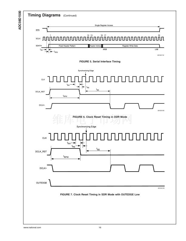
Output Voltage Amplitude and Serial Interface Clock. Tie this
pin high for normal differential DCLK and data amplitude.
Ground this pin for a reduced differential output amplitude and
reduced power consumption. See Section 1.1.6. When the
extended control mode is enabled, this pin functions as the
SCLK input which clocks in the serial data.See Section 1.2 for
details on the extended control mode. See Section 1.3 for
description of the serial interface.
DCLK Edge Select, Double Data Rate Enable and Serial Data
Input. This input sets the output edge of DCLK+ at which the
output data transitions. (See Section 1.1.5.2). When this pin is
floating or connected to 1/2 the supply voltage, DDR clocking
is enabled. When the extended control mode is enabled, this
pin functions as the SDATA input. See Section 1.2 for details
on the extended control mode. See Section 1.3 for description
of the serial interface.
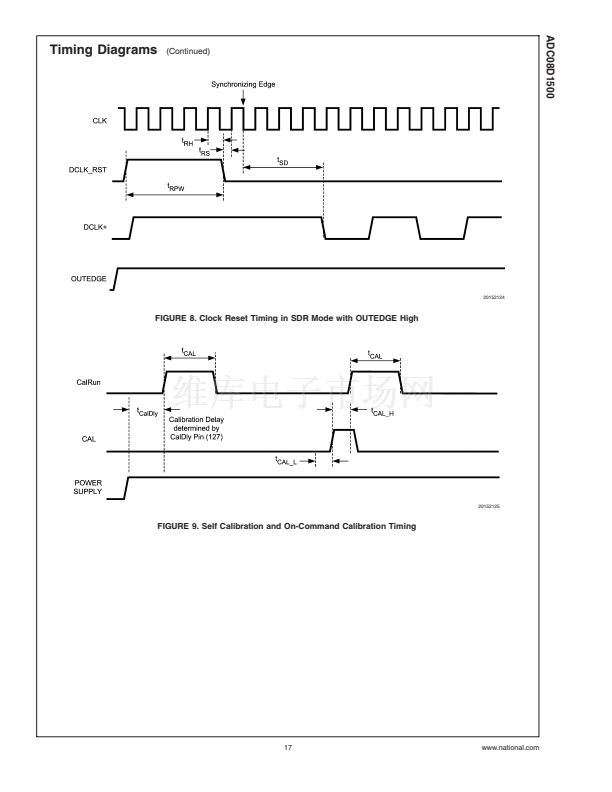
DCLK Reset. A positive pulse on this pin is used to reset and
synchronize the DCLK outs of multiple converters. See
Section 1.5 for detailed description.
Power Down Pins. A logic high on the PD pin puts the entire
device into the Power Down Mode. A logic high on the PDQ
pin puts only the "Q" ADC into the Power Down mode.
Calibration Cycle Initiate. A minimum 80 input clock cycles
logic low followed by a minimum of 80 input clock cycles high
on this pin initiates the self calibration sequence. See Section
2.4.2 for an overview of self-calibration and Section 2.4.2.2 for
a description of on-command calibration.
Full Scale Range Select and Extended Control Enable. In
non-extended control mode, a logic low on this pin sets the
full-scale differential input range to 650 mV
P-P
. A logic high on
this pin sets the full-scale differential input range to 870
mV
P-P
. See Section 1.1.4. To enable the extended control
mode, whereby the serial interface and control registers are
employed, allow this pin to float or connect it to a voltage
equal to V
A
/2. See Section 1.2 for information on the
extended control mode.
Calibration Delay, Dual Edge Sampling and Serial Interface
Chip Select. With a logic high or low on pin 14, this pin
functions as Calibration Delay and sets the number of input
clock cycles after power up before calibration begins (See
Section 1.1.1). With pin 14 floating, this pin acts as the enable
pin for the serial interface input and the CalDly value
becomes "0" (short delay with no provision for a long
power-up calibration delay). When this pin is floating or
connected to a voltage equal to V
A
/2, DES (Dual Edge
Sampling) mode is selected where the "I" input is sampled at
twice the input clock rate and the "Q" input is ignored. See
Section 1.1.5.1.
3
OutV / SCLK
4
OutEdge / DDR
/ SDATA
15
DCLK_RST
26
29
PD
PDQ
30
CAL
14
FSR/ECE
127
CalDly / DES /
SCS
3
www.national.com


 1
1
 2
2
 3
3
 4
4
 5
5
 6
6
 7
7
 8
8
 9
9
 10
10
 11
11
 12
12
 13
13
 14
14
 15
15
 16
16
 17
17
 18
18
 19
19
 20
20
 21
21
 22
22
 23
23
 24
24
 25
25
 26
26
 27
27
 28
28
 29
29
 30
30
 31
31
 32
32
 33
33
