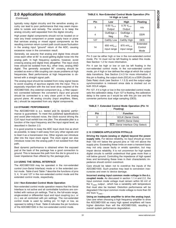
.
Q鈭?/div>
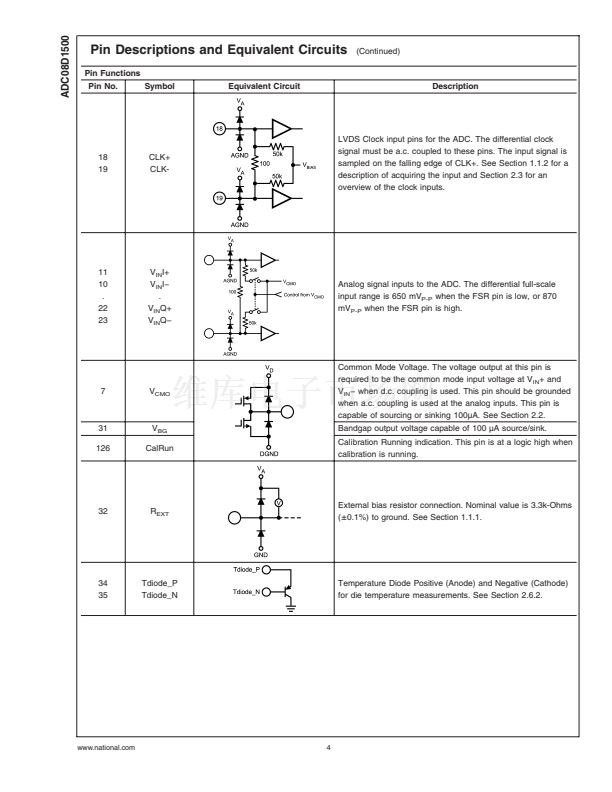
Analog signal inputs to the ADC. The differential full-scale
input range is 650 mV
P-P
when the FSR pin is low, or 870
mV
P-P
when the FSR pin is high.
7
V
CMO
Common Mode Voltage. The voltage output at this pin is
required to be the common mode input voltage at V
IN
+ and
V
IN
鈭?when d.c. coupling is used. This pin should be grounded
when a.c. coupling is used at the analog inputs. This pin is
capable of sourcing or sinking 100碌A. See Section 2.2.
Bandgap output voltage capable of 100 碌A source/sink.
Calibration Running indication. This pin is at a logic high when
calibration is running.
31
126
V
BG
CalRun
32
R
EXT
External bias resistor connection. Nominal value is 3.3k-Ohms
(
卤
0.1%) to ground. See Section 1.1.1.
34
35
Tdiode_P
Tdiode_N
Temperature Diode Positive (Anode) and Negative (Cathode)
for die temperature measurements. See Section 2.6.2.
www.national.com
4


 1
1
 2
2
 3
3
 4
4
 5
5
 6
6
 7
7
 8
8
 9
9
 10
10
 11
11
 12
12
 13
13
 14
14
 15
15
 16
16
 17
17
 18
18
 19
19
 20
20
 21
21
 22
22
 23
23
 24
24
 25
25
 26
26
 27
27
 28
28
 29
29
 30
30
 31
31
 32
32
 33
33
