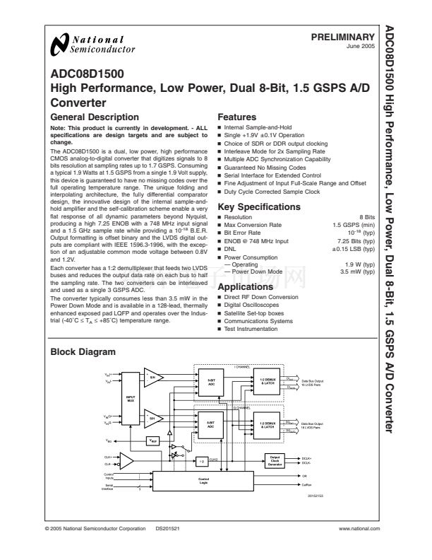
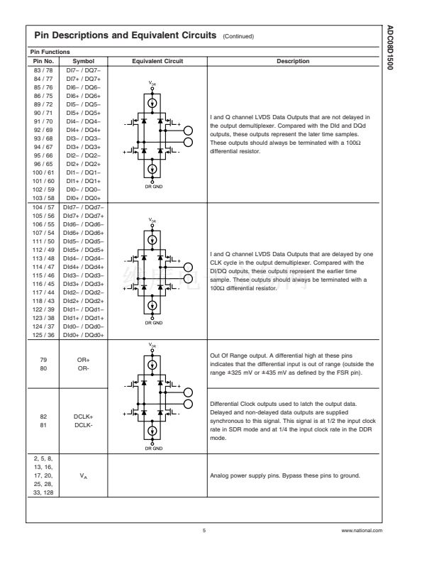
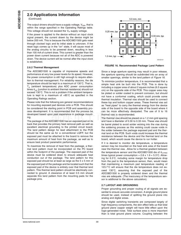
the output demultiplexer. Compared with the DId and DQd
outputs, these outputs represent the later time samples.
These outputs should always be terminated with a 100鈩?/div>
differential resistor.
I and Q channel LVDS Data Outputs that are delayed by one
CLK cycle in the output demultiplexer. Compared with the
DI/DQ outputs, these outputs represent the earlier time
sample. These outputs should always be terminated with a
100鈩?differential resistor.
79
80
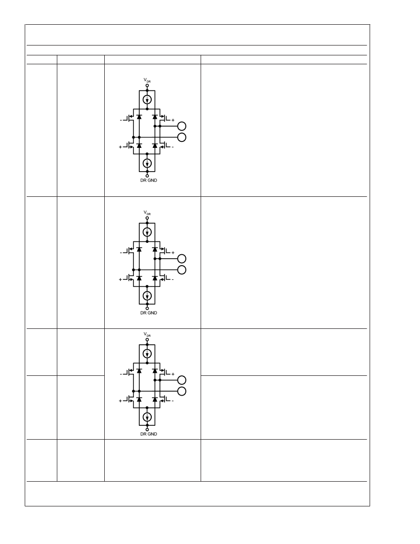
OR+
OR-
Out Of Range output. A differential high at these pins
indicates that the differential input is out of range (outside the
range
卤
325 mV or
卤
435 mV as defined by the FSR pin).
82
81
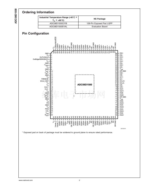
DCLK+
DCLK-
Differential Clock outputs used to latch the output data.
Delayed and non-delayed data outputs are supplied
synchronous to this signal. This signal is at 1/2 the input clock
rate in SDR mode and at 1/4 the input clock rate in the DDR
mode.
2, 5, 8,
13, 16,
17, 20,
25, 28,
33, 128
V
A
Analog power supply pins. Bypass these pins to ground.
5
www.national.com


 1
1
 2
2
 3
3
 4
4
 5
5
 6
6
 7
7
 8
8
 9
9
 10
10
 11
11
 12
12
 13
13
 14
14
 15
15
 16
16
 17
17
 18
18
 19
19
 20
20
 21
21
 22
22
 23
23
 24
24
 25
25
 26
26
 27
27
 28
28
 29
29
 30
30
 31
31
 32
32
 33
33
