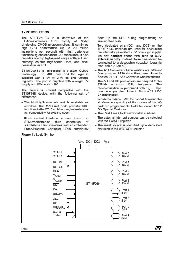
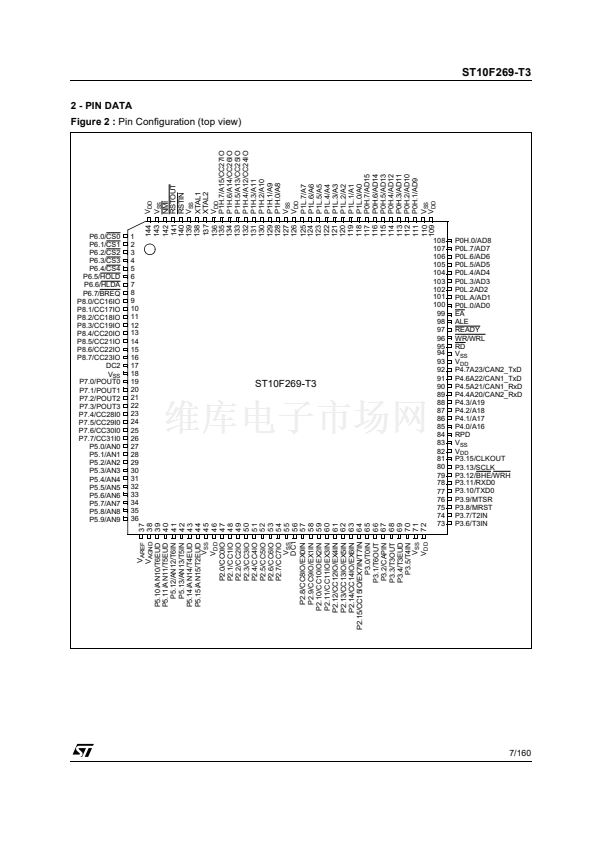
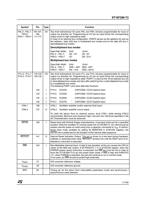
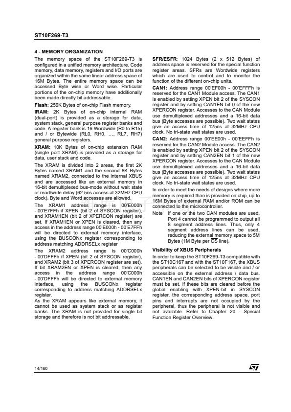
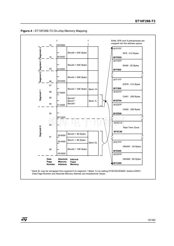
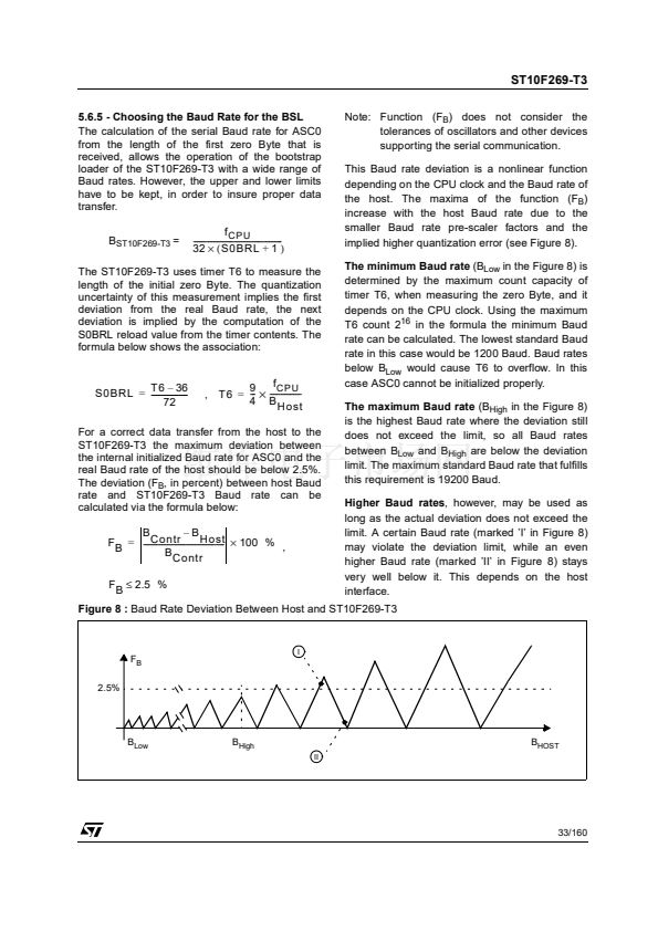
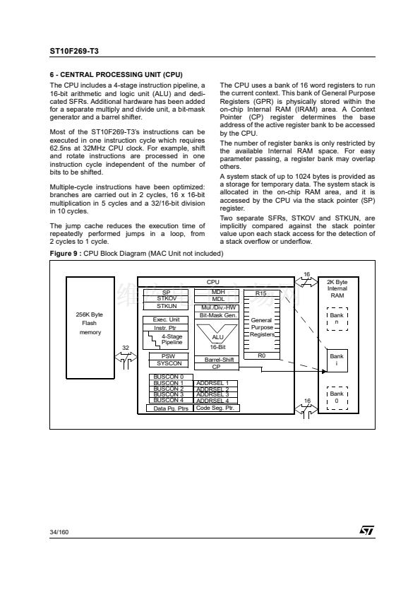
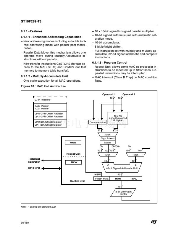
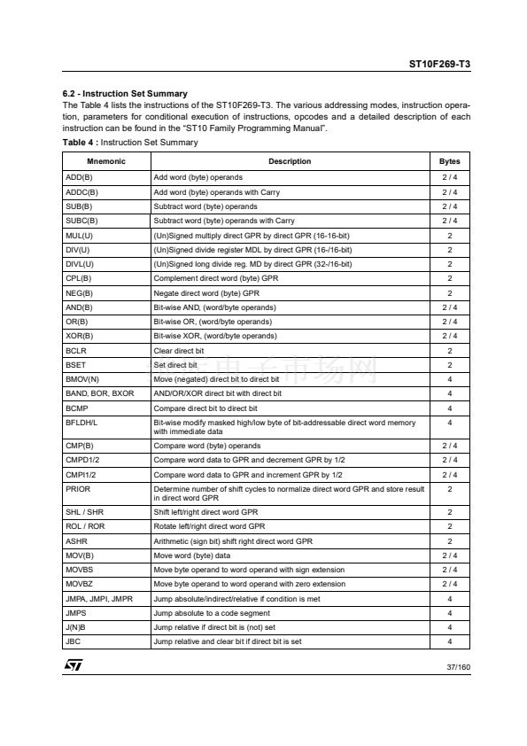
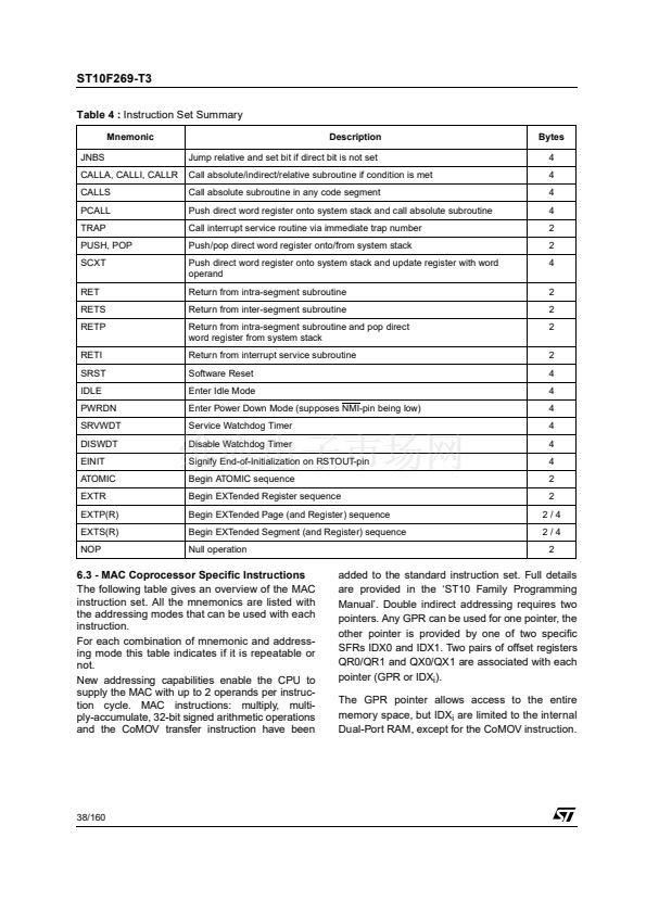
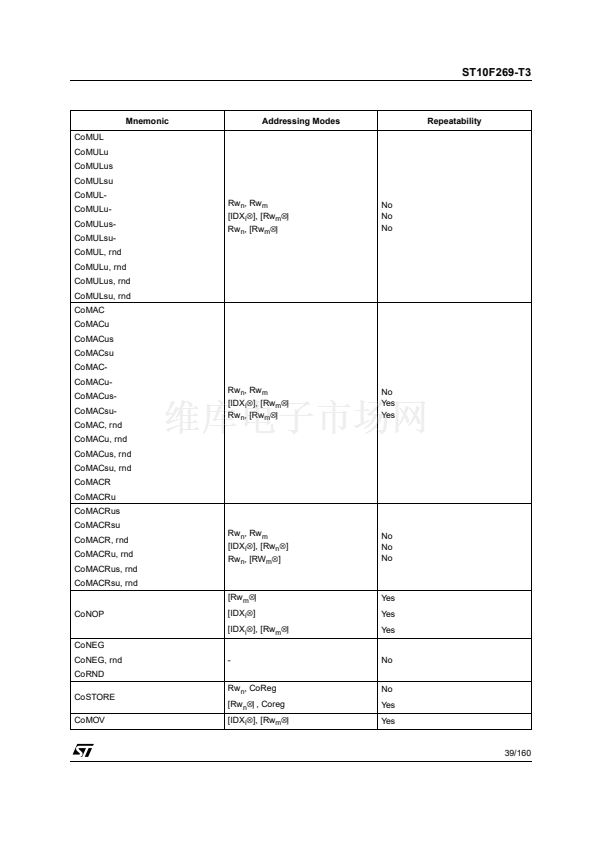
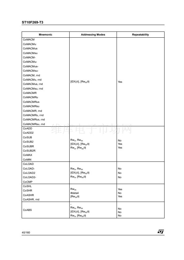
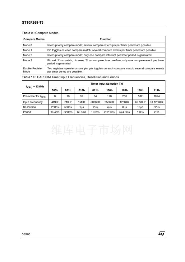
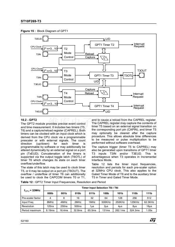
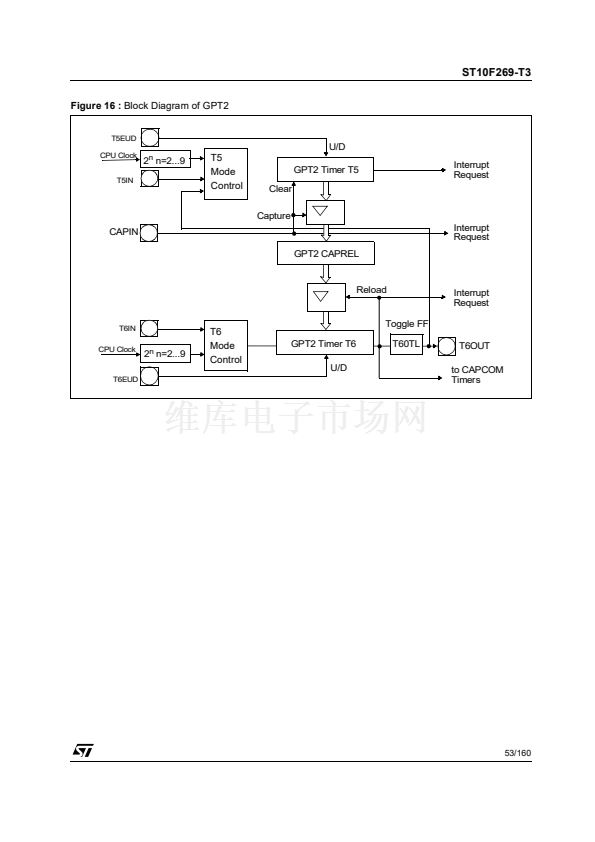
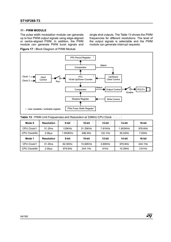
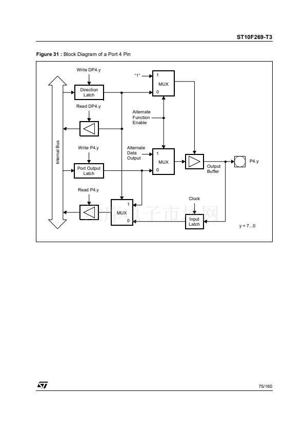
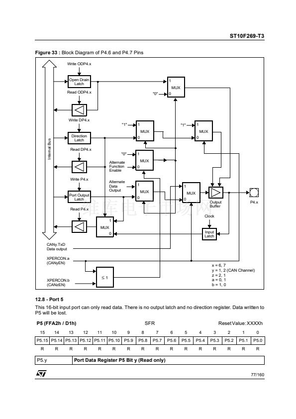
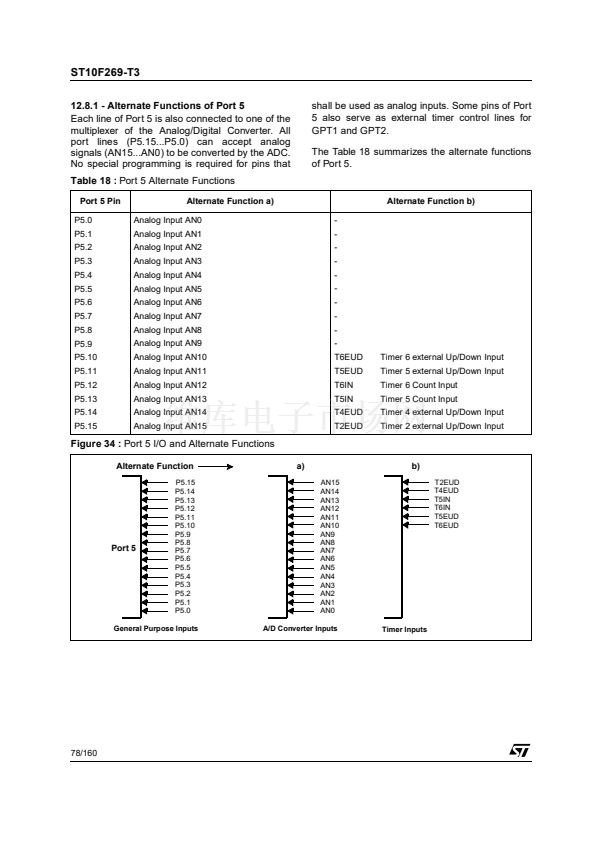
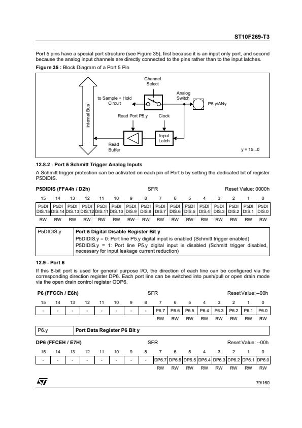
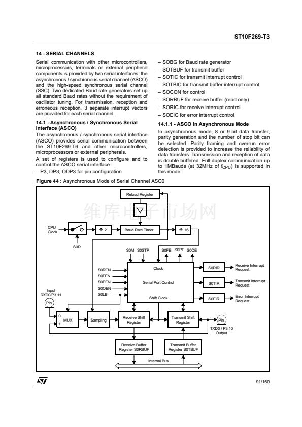
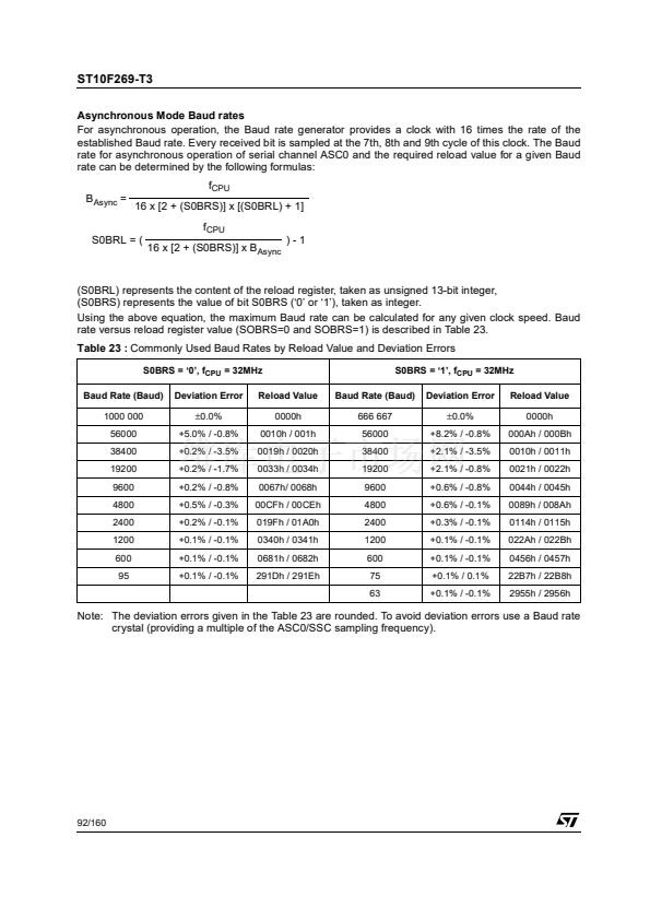
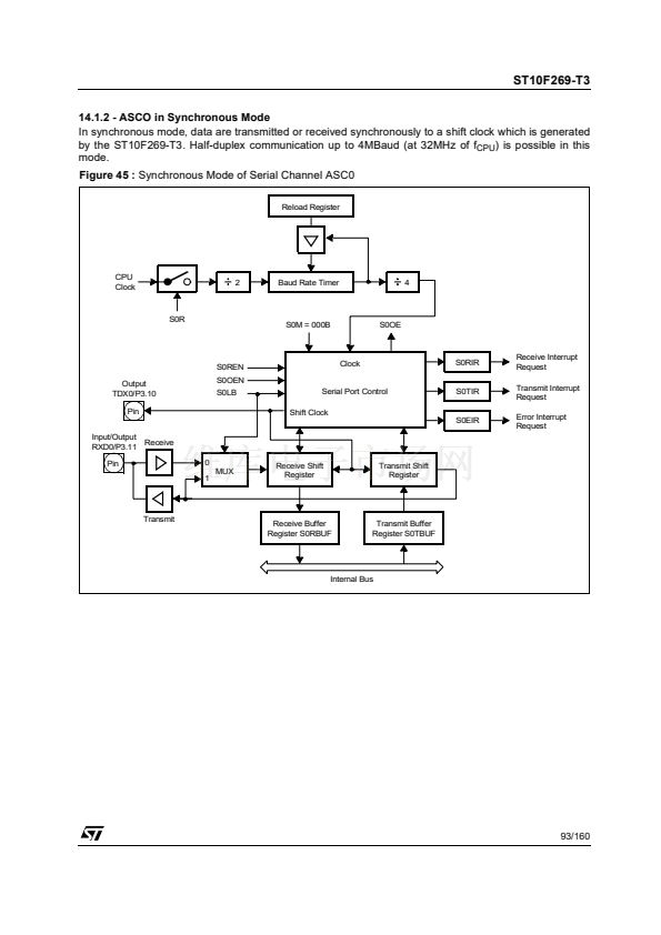
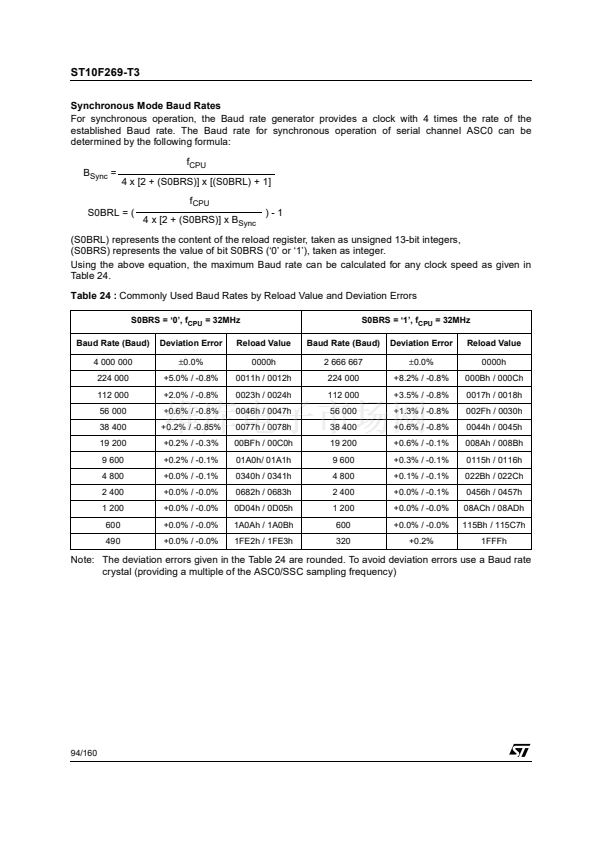
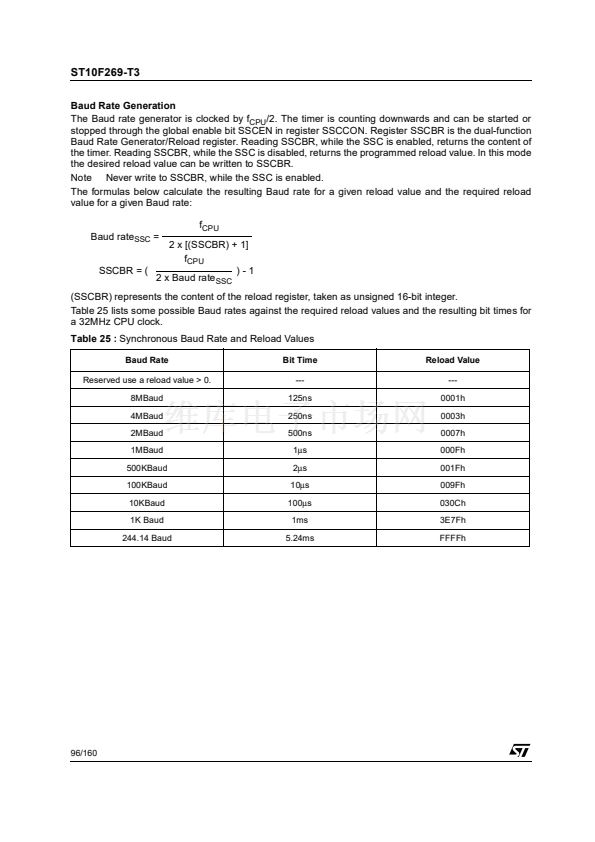
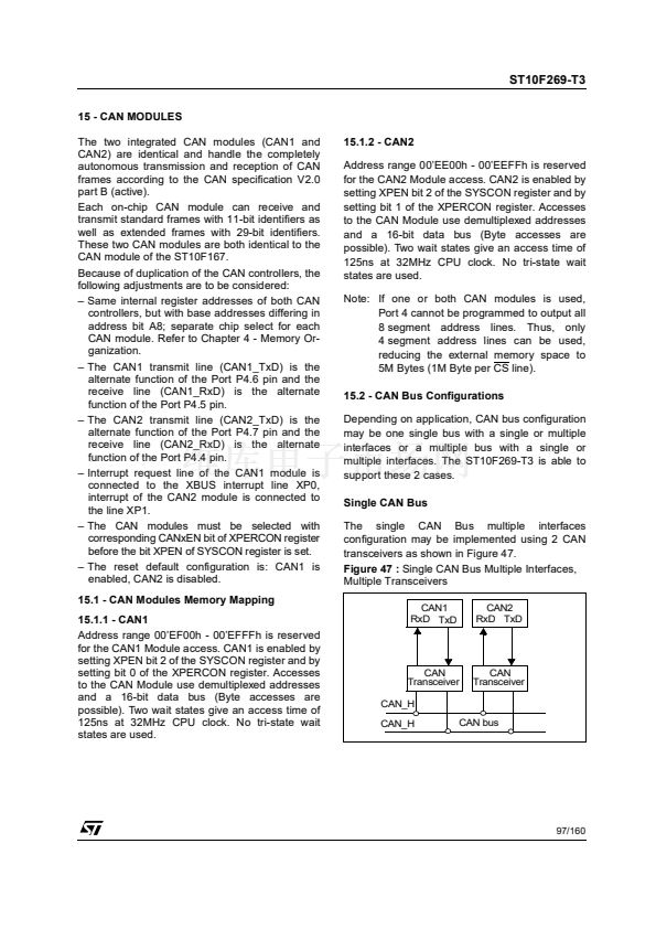
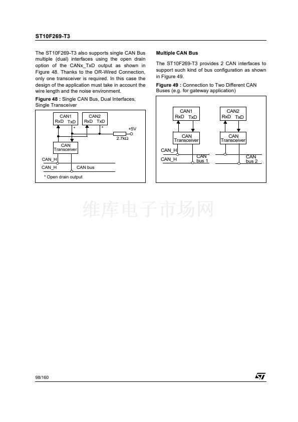
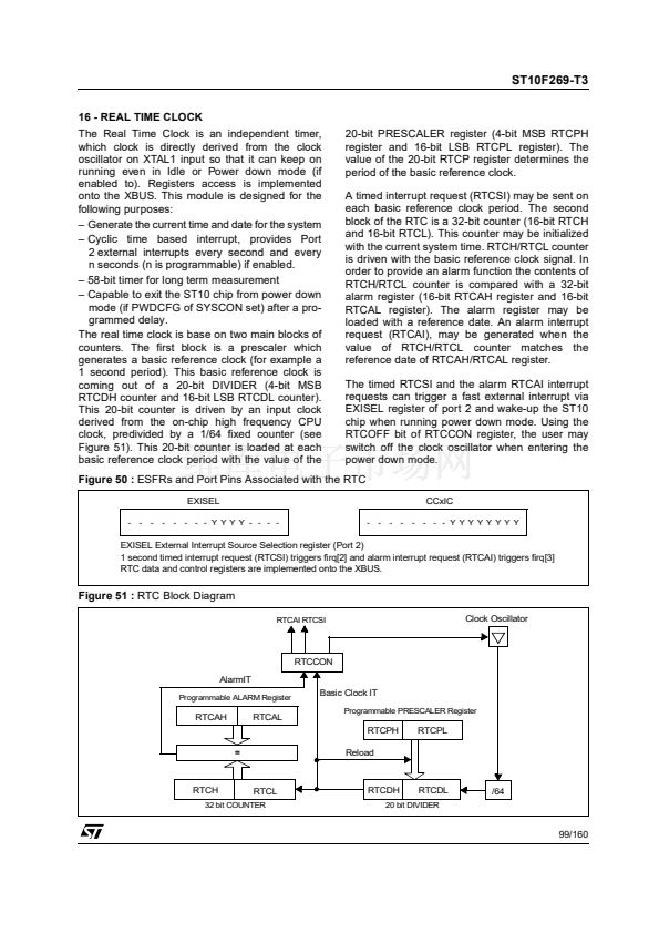
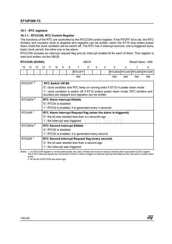
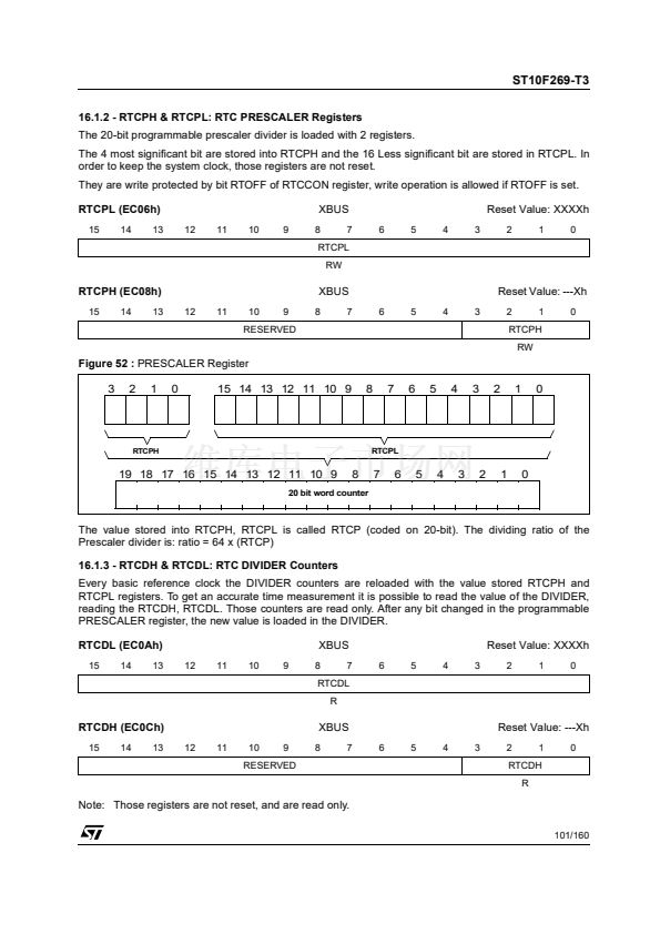
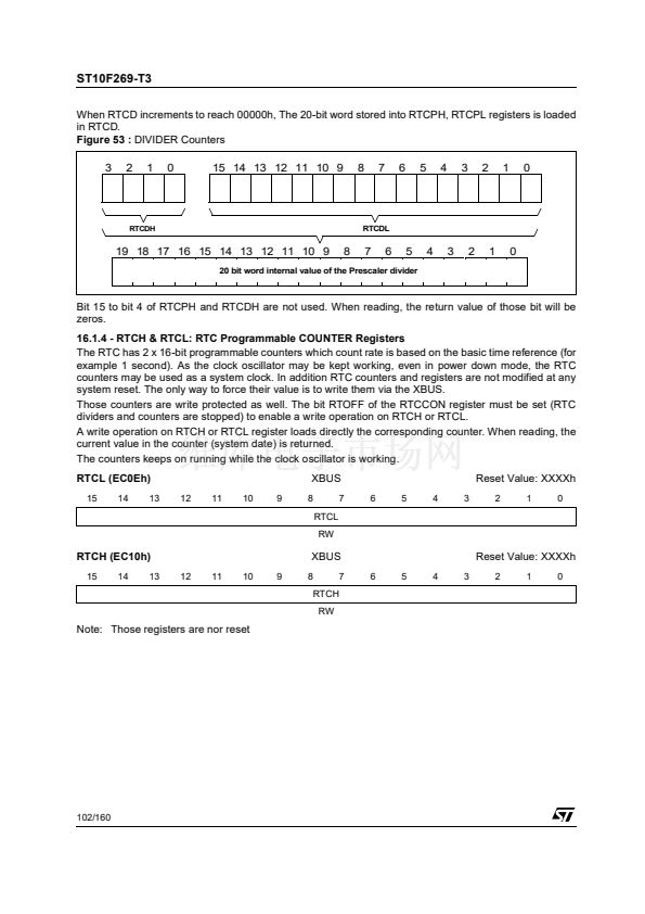
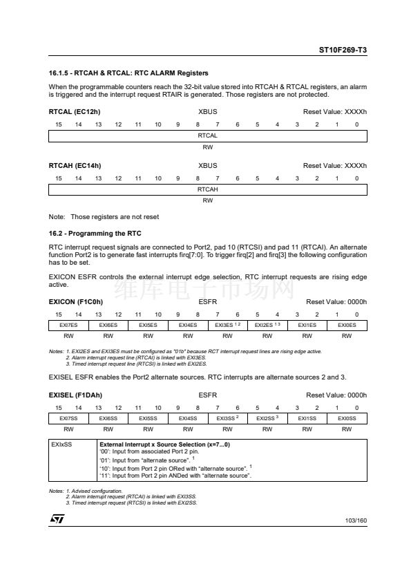
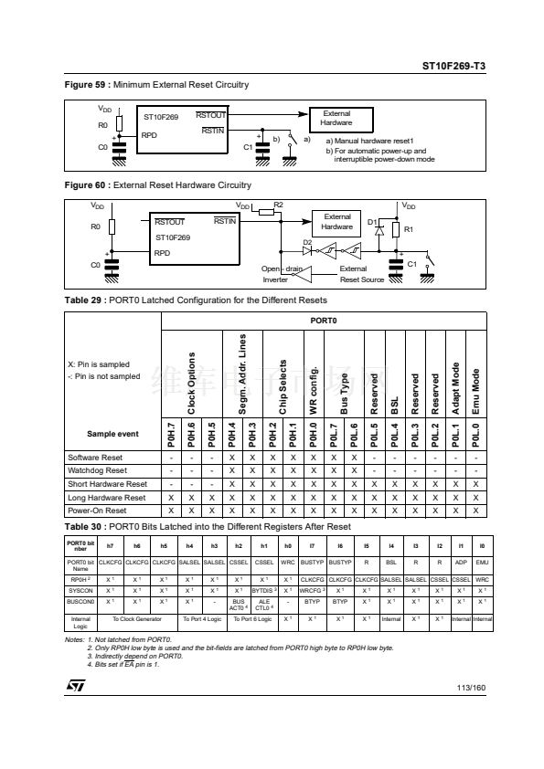
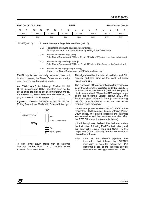
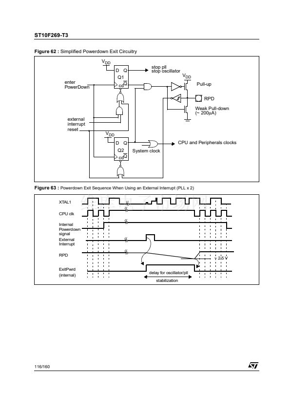
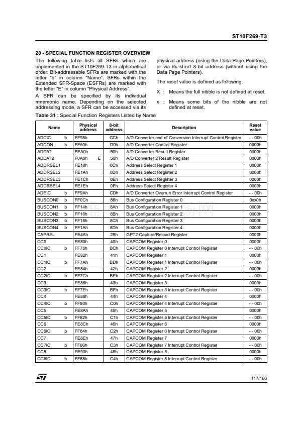
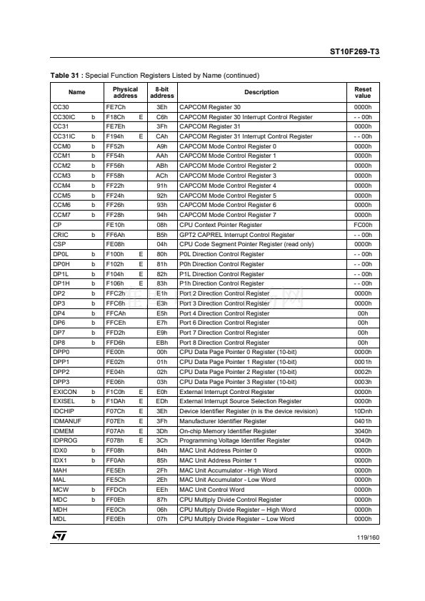
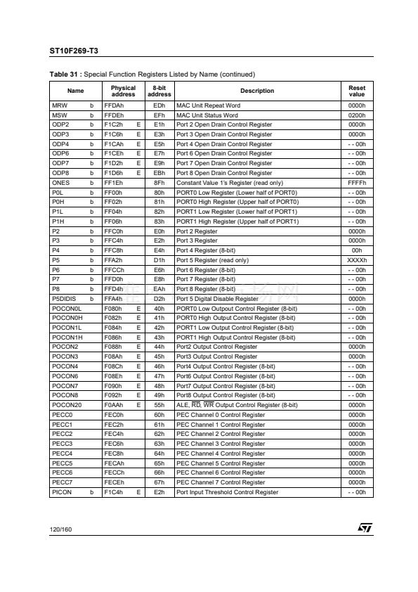
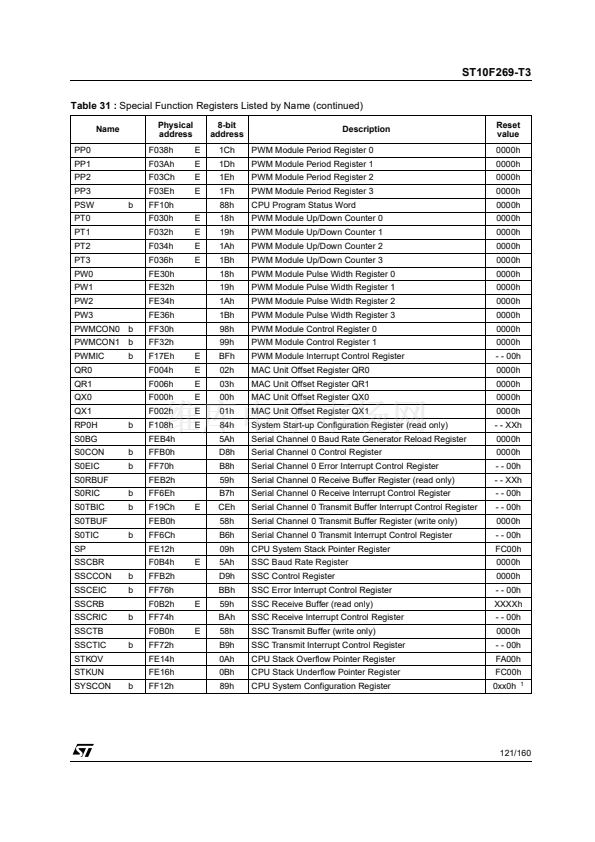
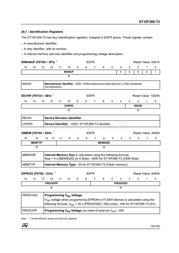
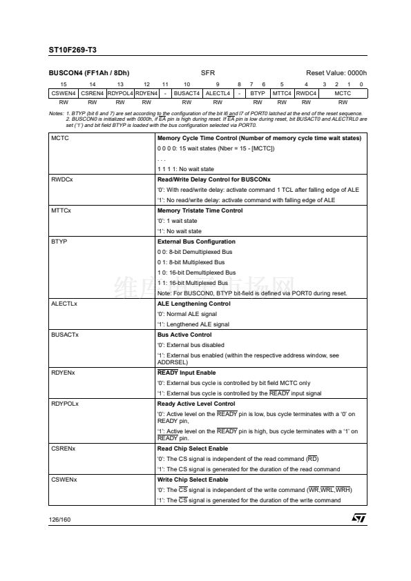
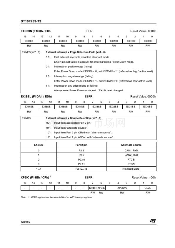
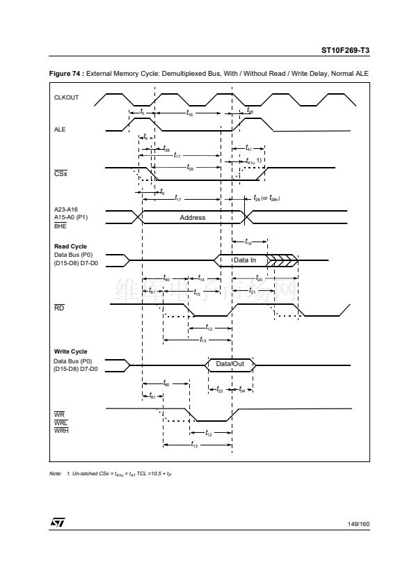
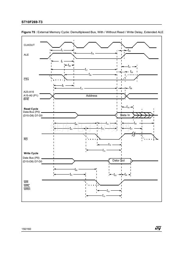
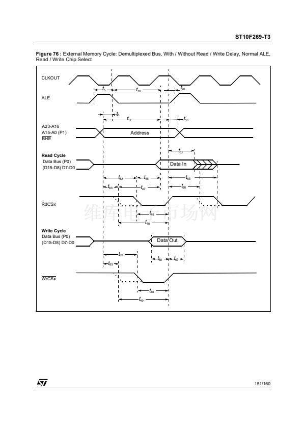
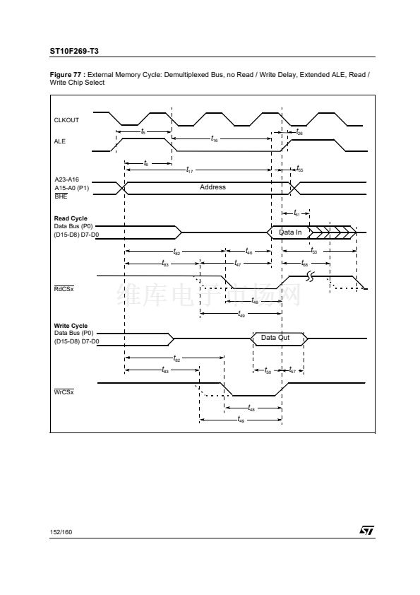
ST10F269-T3
Table 7 :
Interrupt Sources (continued)
Source of Interrupt or PEC
Service Request
CAPCOM Timer 1
CAPCOM Timer 7
CAPCOM Timer 8
GPT1 Timer 2
GPT1 Timer 3
GPT1 Timer 4
GPT2 Timer 5
GPT2 Timer 6
GPT2 CAPREL Register
A/D Conversion Complete
A/D Overrun Error
ASC0 Transmit
ASC0 Transmit Buffer
ASC0 Receive
ASC0 Error
SSC Transmit
SSC Receive
SSC Error
PWM Channel 0...3
CAN1 Interface
CAN2 Interface
FLASH Ready / Busy
PLL Unlock/OWD
Request
Flag
T1IR
T7IR
T8IR
T2IR
T3IR
T4IR
T5IR
T6IR
CRIR
ADCIR
ADEIR
S0TIR
S0TBIR
S0RIR
S0EIR
SCTIR
SCRIR
SCEIR
PWMIR
XP0IR
XP1IR
XP2IR
XP3IR
Enable
Flag
T1IE
T7IE
T8IE
T2IE
T3IE
T4IE
T5IE
T6IE
CRIE
ADCIE
ADEIE
S0TIE
S0TBIE
S0RIE
S0EIE
SCTIE
SCRIE
SCEIE
PWMIE
XP0IE
XP1IE
XP2IE
XP3IE
Interrupt
Vector
T1INT
T7INT
T8INT
T2INT
T3INT
T4INT
T5INT
T6INT
CRINT
ADCINT
ADEINT
S0TINT
S0TBINT
S0RINT
S0EINT
SCTINT
SCRINT
SCEINT
PWMINT
XP0INT
XP1INT
XP2INT
XP3INT
Vector
Location
00鈥?084h
00鈥?0F4h
00鈥?0F8h
00鈥?088h
00鈥?08Ch
00鈥?090h
00鈥?094h
00鈥?098h
00鈥?09Ch
00鈥?0A0h
00鈥?0A4h
00鈥?0A8h
00鈥?11Ch
00鈥?0ACh
00鈥?0B0h
00鈥?0B4h
00鈥?0B8h
00鈥?0BCh
00鈥?0FCh
00鈥?100h
00鈥?104h
00鈥?108h
00鈥?10Ch
Trap
Number
21h
3Dh
3Eh
22h
23h
24h
25h
26h
27h
28h
29h
2Ah
47h
2Bh
2Ch
2Dh
2Eh
2Fh
3Fh
40h
41h
42h
43h
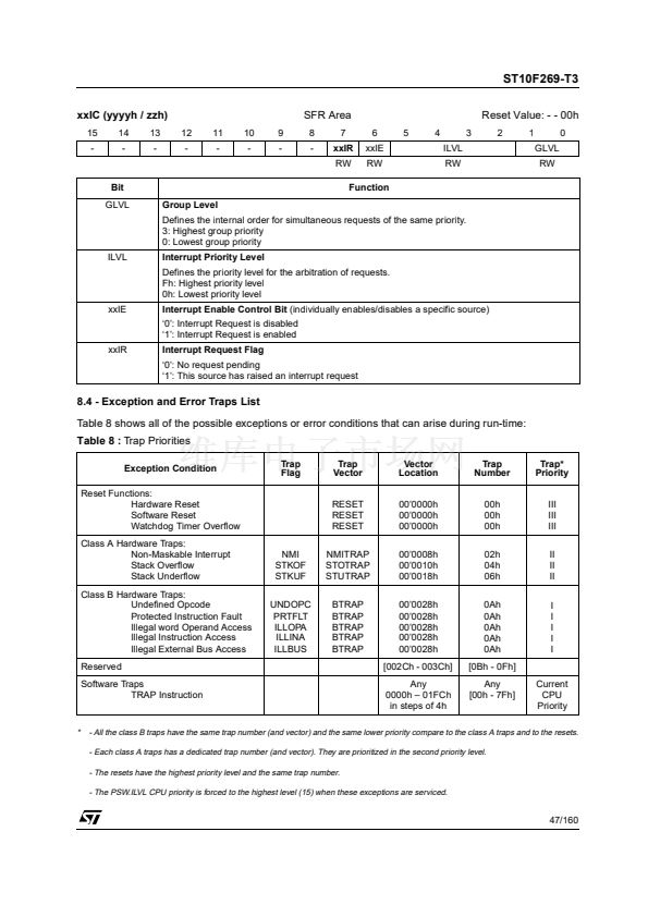
Hardware traps are exceptions or error conditions
that arise during run-time. They cause immediate
non-maskable system reaction similar to a
standard interrupt service (branching to a
dedicated vector table location).
The occurrence of a hardware trap is additionally
signified by an individual bit in the trap flag
register (TFR). Except when another higher
prioritized trap service is in progress, a hardware
trap will interrupt any other program execution.
Hardware trap services cannot not be interrupted
by standard interrupt or by PEC interrupts.
8.3 - Interrupt Control Registers
All interrupt control registers are identically
organized. The lower 8 bits of an interrupt control
register contain the complete interrupt status
information of the associated source, which is
46/160
required during one round of prioritization, the
upper 8 bits of the respective register are
reserved. All interrupt control registers are bit
addressable and all bits can be read or written via
software.
This allows each interrupt source to be
programmed or modified with just one instruction.
When accessing interrupt control registers
through instructions which operate on Word data
types, their upper 8 bits (15...8) will return zeros,
when read, and will discard written data.
The layout of the Interrupt Control registers shown
below applies to each xxIC register, where xx
stands for the mnemonic for the respective
source.


 1
1
 2
2
 3
3
 4
4
 5
5
 6
6
 7
7
 8
8
 9
9
 10
10
 11
11
 12
12
 13
13
 14
14
 15
15
 16
16
 17
17
 18
18
 19
19
 20
20
 21
21
 22
22
 23
23
 24
24
 25
25
 26
26
 27
27
 28
28
 29
29
 30
30
 31
31
 32
32
 33
33
 34
34
 35
35
 36
36
 37
37
 38
38
 39
39
 40
40
 41
41
 42
42
 43
43
 44
44
 45
45
 46
46
 47
47
 48
48
 49
49
 50
50
 51
51
 52
52
 53
53
 54
54
 55
55
 56
56
 57
57
 58
58
 59
59
 60
60
 61
61
 62
62
 63
63
 64
64
 65
65
 66
66
 67
67
 68
68
 69
69
 70
70
 71
71
 72
72
 73
73
 74
74
 75
75
 76
76
 77
77
 78
78
 79
79
 80
80
 81
81
 82
82
 83
83
 84
84
 85
85
 86
86
 87
87
 88
88
 89
89
 90
90
 91
91
 92
92
 93
93
 94
94
 95
95
 96
96
 97
97
 98
98
 99
99
 100
100
 101
101
 102
102
 103
103
 104
104
 105
105
 106
106
 107
107
 108
108
 109
109
 110
110
 111
111
 112
112
 113
113
 114
114
 115
115
 116
116
 117
117
 118
118
 119
119
 120
120
 121
121
 122
122
 123
123
 124
124
 125
125
 126
126
 127
127
 128
128
 129
129
 130
130
 131
131
 132
132
 133
133
 134
134
 135
135
 136
136
 137
137
 138
138
 139
139
 140
140
 141
141
 142
142
 143
143
 144
144
 145
145
 146
146
 147
147
 148
148
 149
149
 150
150
 151
151
 152
152
 153
153
 154
154
 155
155
 156
156
 157
157
 158
158
 159
159
 160
160
