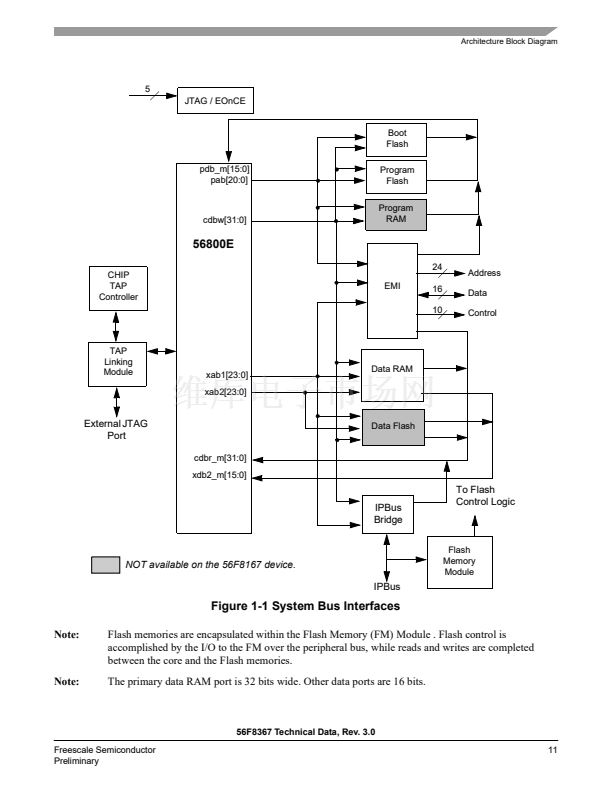
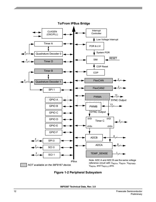
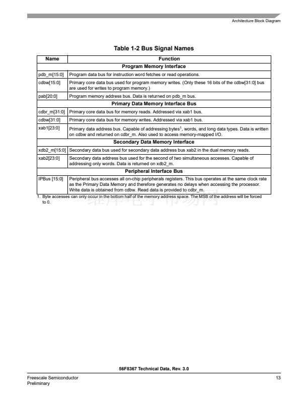
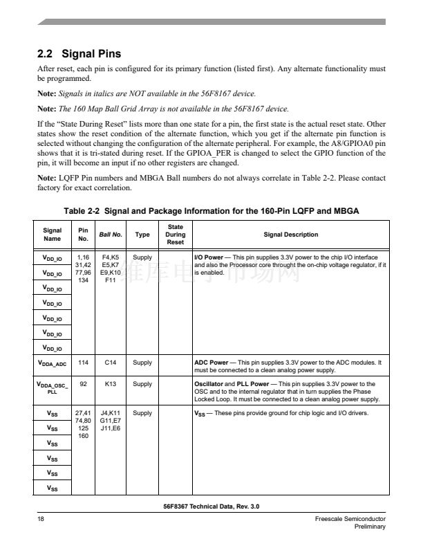
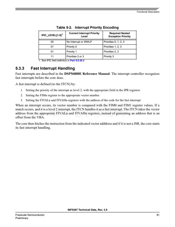
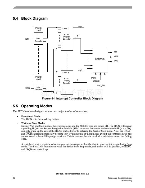
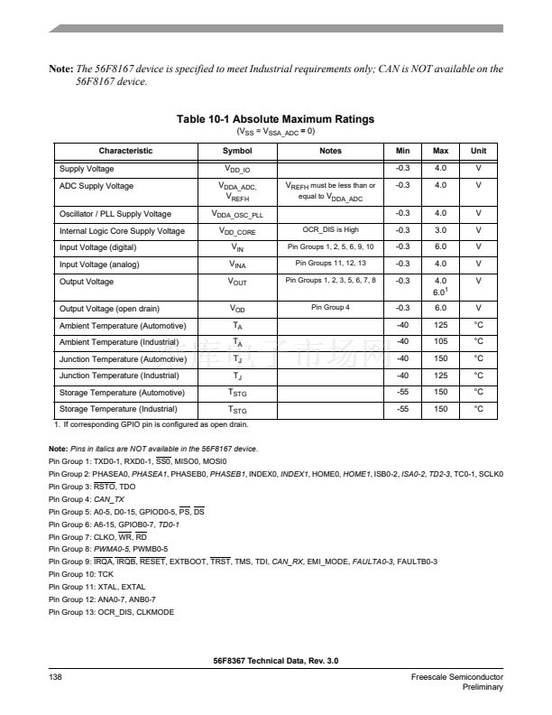
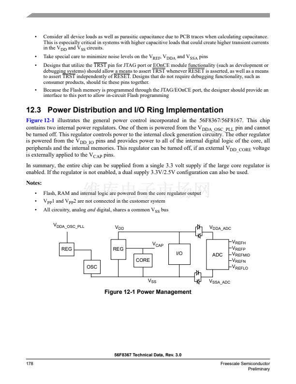
Power
Power
Power
Ground
Ground
V
DD_IO
V
DDA_OSC_PLL
V
DDA_ADC
V
SS
V
SSA_ADC
OCR_DIS
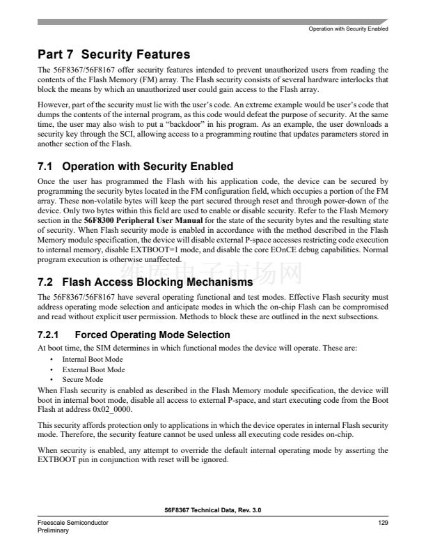
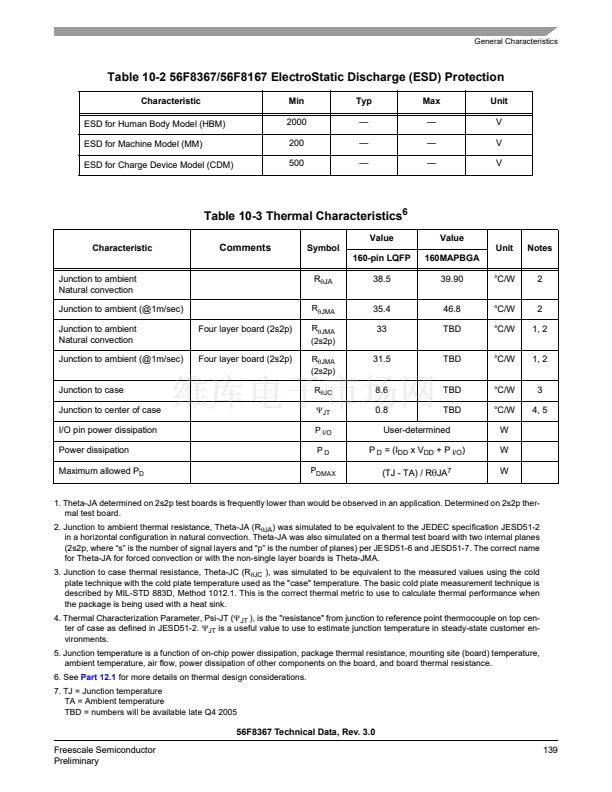
7
1
1
6
1
1
4
2
1
1
1
1
6
2
8
8
1
1
1
1
7
9
1
1
1
1
1
1
1
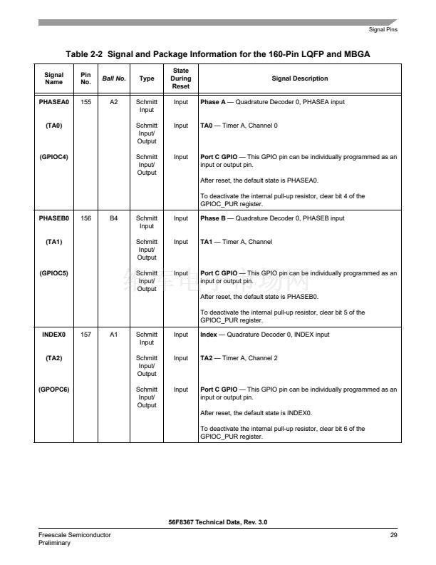
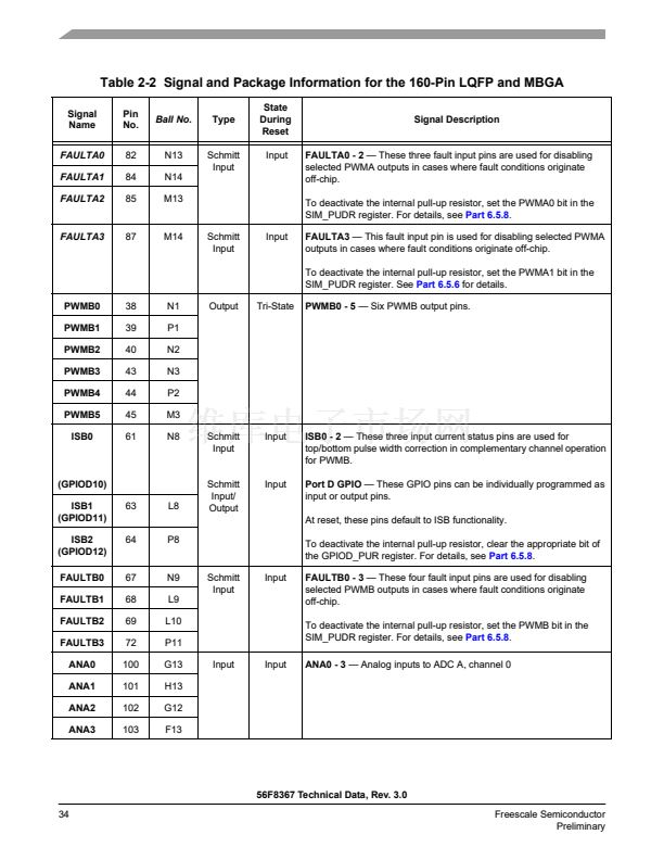
PHASEA0 (TA0, GPIOC4)
PHASEB0 (TA1, GPIOC5)
INDEX0 (TA2, GPIOC6)
HOME0 (TA3, GPIOC7)
SCLK0
MOSI0 (GPIOE5)
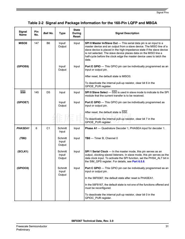
MISO0 (GPIOE6)
SS0 (GPIOE7)
PHASEA1(TB0, SCLK1, GPIOC0)
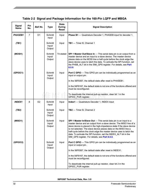
PHASEB1 (TB1, MOSI1, GPIOC1)
INDEX1 (TB2, MISO1, GPIOC2)
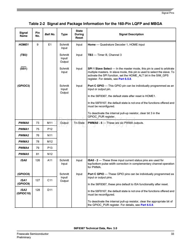
HOME1 (TB3, SS1, GPIOC3)
PWMA0 - 5
ISA0 - 2 (GPIOC8 - 10)
FAULTA0 - 3
Quadrature
Decoder 0
or Quad
Timer A
56F8367
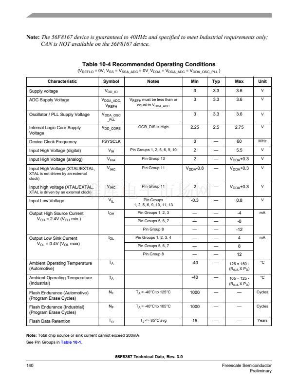
1
1
1
1
1
1
1
1
6
3
4
Other
Supply
Ports
PLL
and
Clock
*V
CAP
1 - V
CAP
4
V
PP
1 & V
PP
2
CLKMODE
EXTAL
XTAL
CLKO
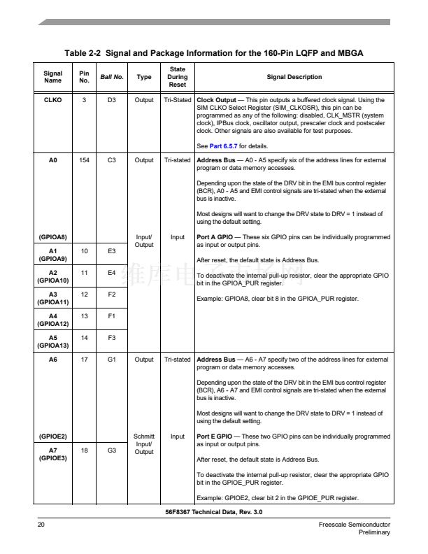
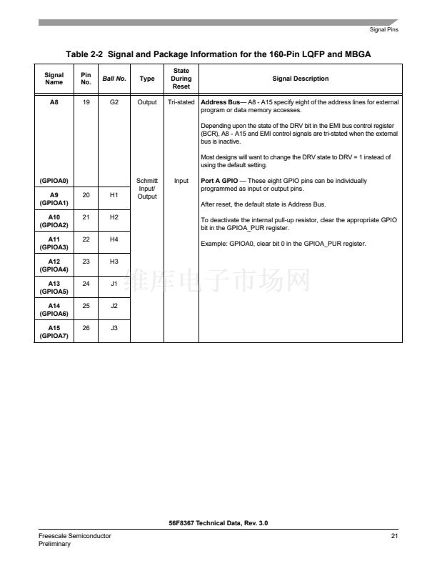
A0 - A5 (GPIOA8 - 13)
A6 - A7 (GPIOE2 - 3)
A8 - A15 (GPIOA0 - 7)
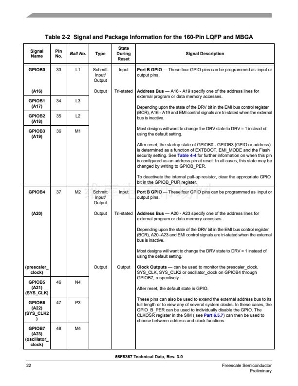
GPIOB0 - 7 (A16 - 23)
GPIOB4 (A20, prescaler_clock)
GPIOB5 (A21, SYS_CLK)
GPIOB6 (A22, SYS_CLK2)
GPIOB7 (A23, oscillator_clock)
SPI0 or
GPIO
Quadrature
Decoder 1 or
Quad Timer B
or SPI 1 or
GPIO
External
Address
Bus
or GPIO
PWMA
6
3
4
PWMB0 - 5
ISB0 - 2 (GPIOD10 - 12)
FAULTB0 - 3
PWMB
External
Data Bus
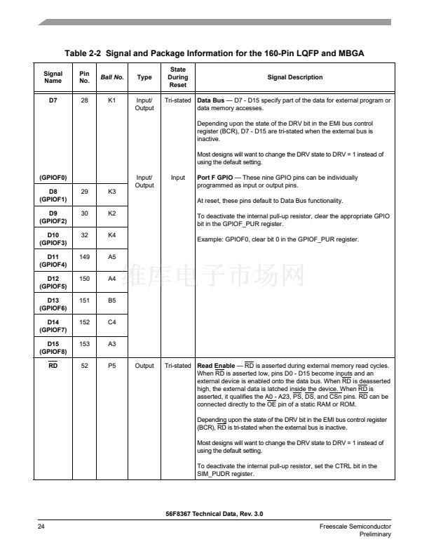
D0 - D6 (GPIOF9 - 15)
D7 - D15 (GPIOF0 - 8)
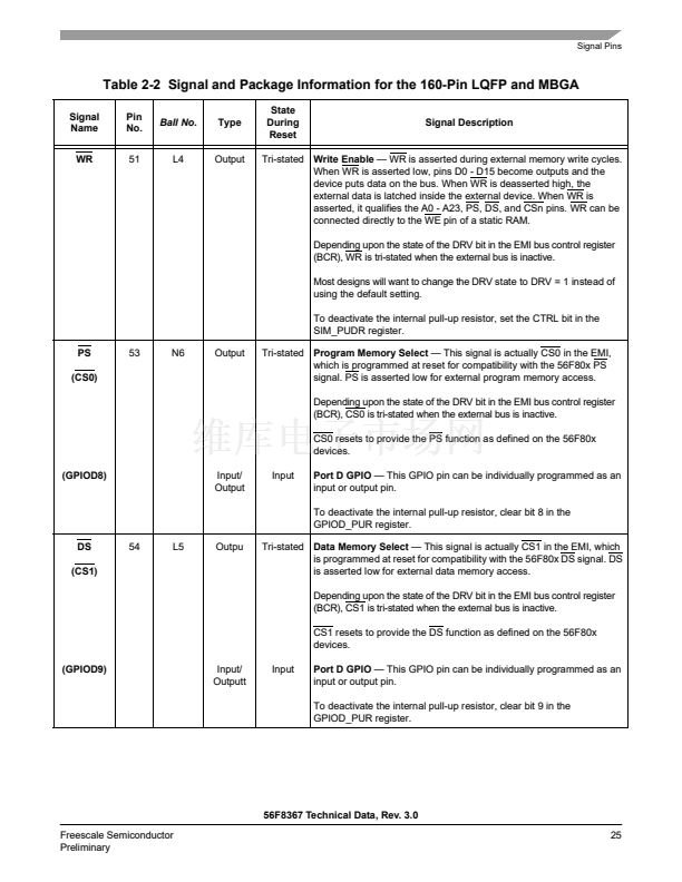
RD
WR
PS/CS0 (GPIODF8)
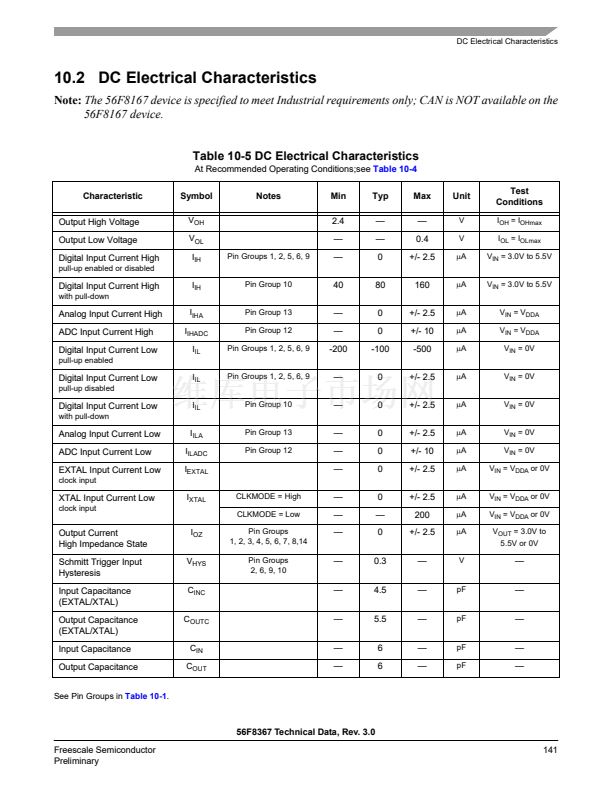
8
5
8
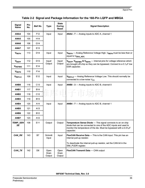
ANA0 - 7
V
REF
ANB0 - 7
ADCA
ADCB
External
Bus
Control
1
Temp_Sense
Temperature
Sense
DS/CS1 (GPIOFD9)
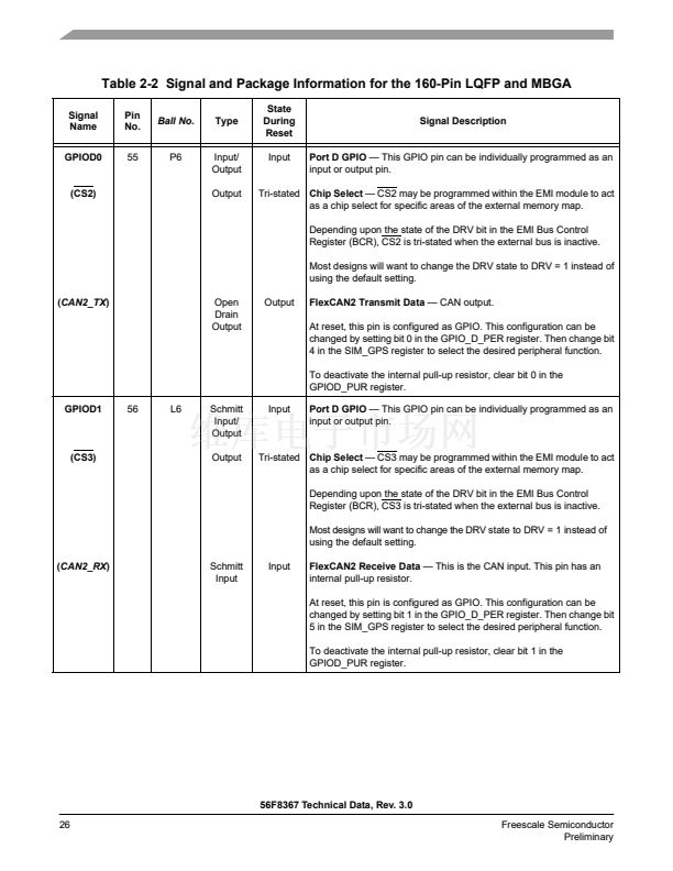
GPIOD0 (CS2, CAN2_TX)
GPIOD1 (CS3, CAN2_RX)
GPIOD2 - 5 (CS4 - 7)
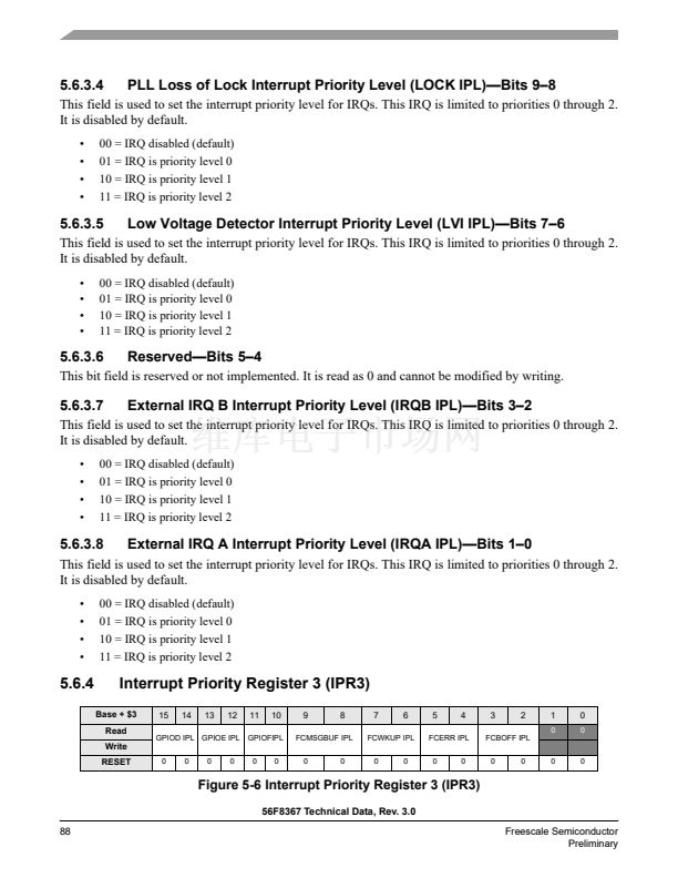
1
1
1
4
1
1
1
1
1
1
1
1
1
2
4
1
1
CAN_RX
CAN_TX
FlexCAN
SCI 0 or
GPIO
SCI 1 or
GPIOD
TXD0 (GPIOE0)
RXD0 (GPIOE1)
TXD1 (GPIOD6)
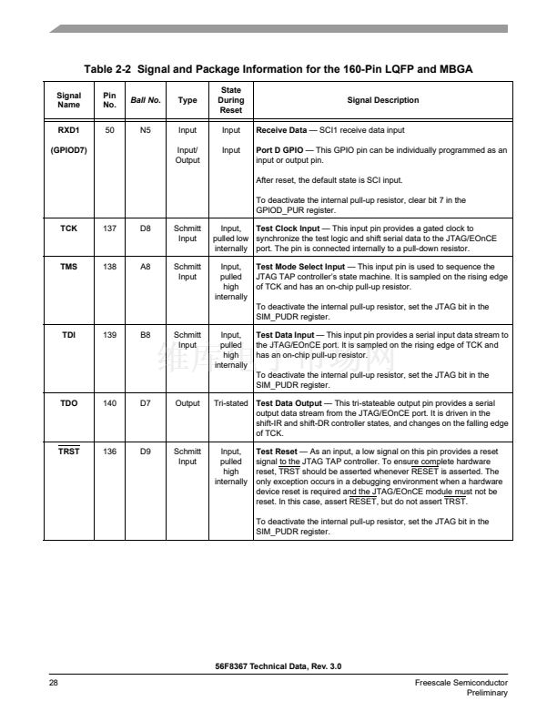
RXD1 (GPIOD7)
TCK
TMS
TDI
TDO
TRST
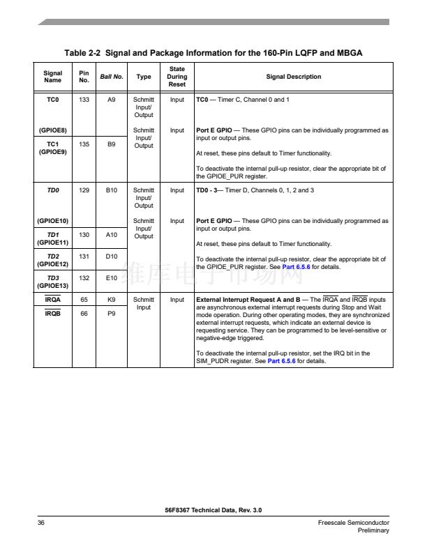
TC0 - 1 (GPIOE8 - 9)
TD0 - 3 (GPIOE10 - 13)
Quad Timer
C and D or
GPIO
1
1
1
1
1
1
IRQA
IRQB
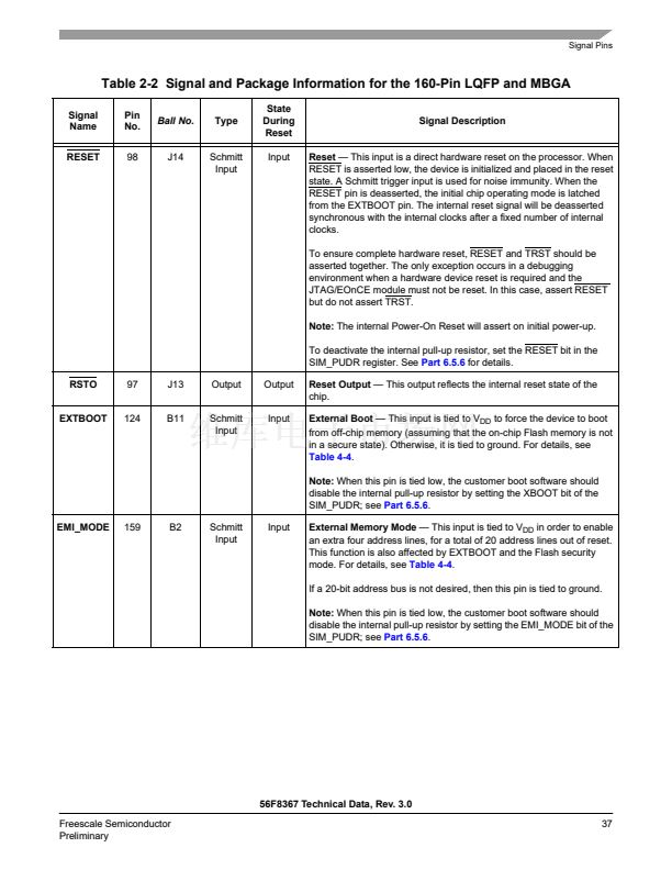
EXTBOOT
EMI_MODE
RESET
RSTO
INTERRUPT/
PROGRAM
CONTROL
JTAG/
EOnCE
Port
* When the on-chip regulator is disabled, these four pins become 2.5V V
DD_CORE
.
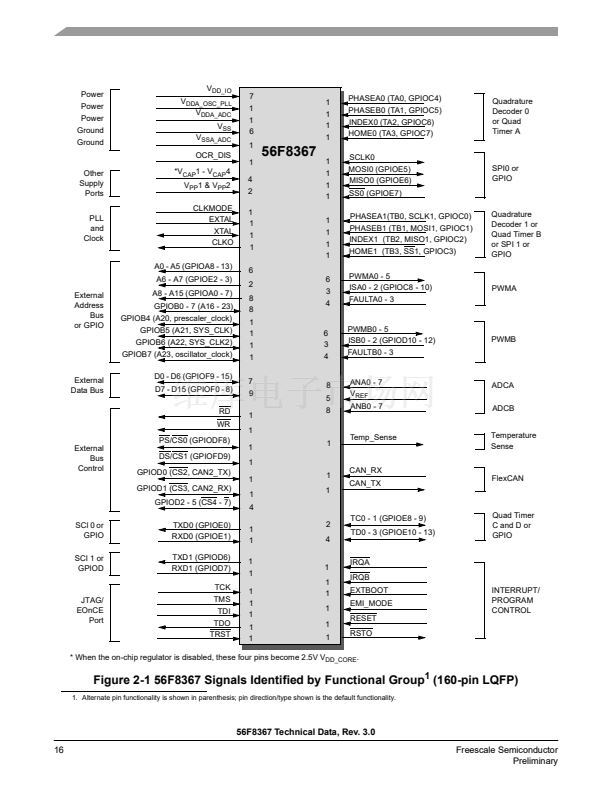
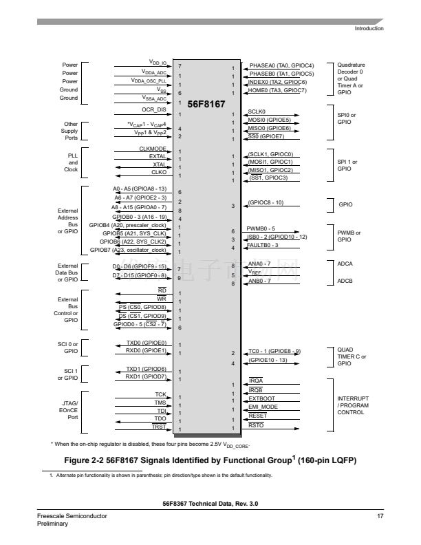
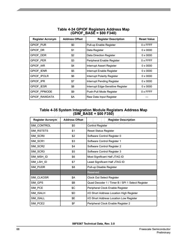
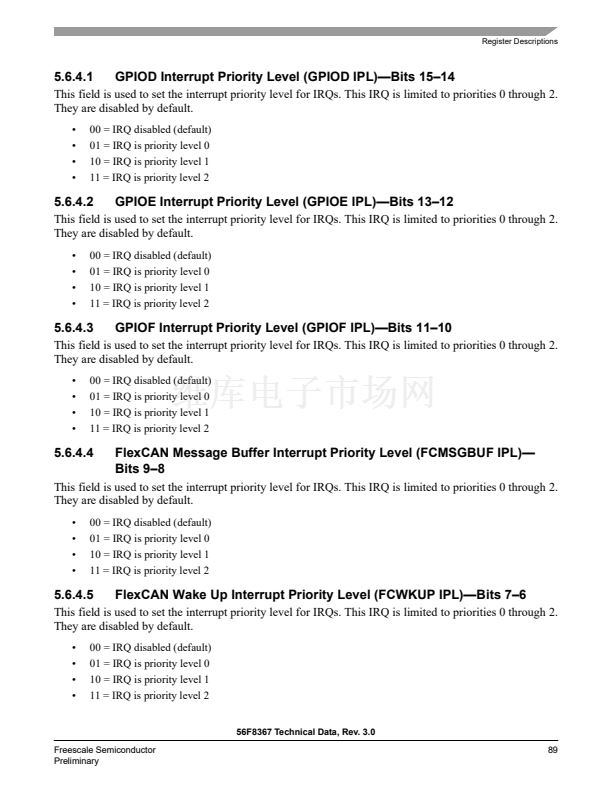
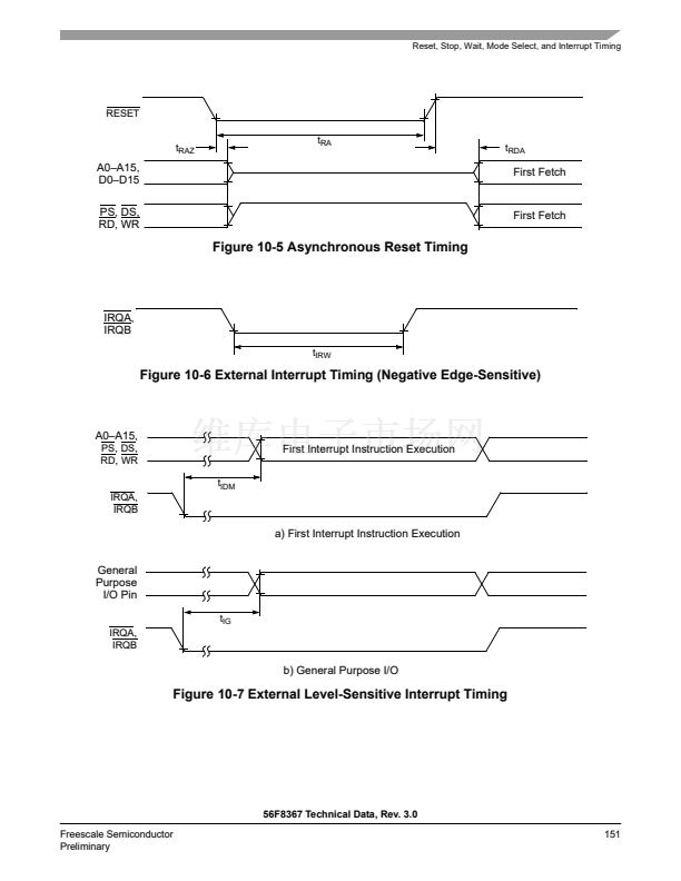
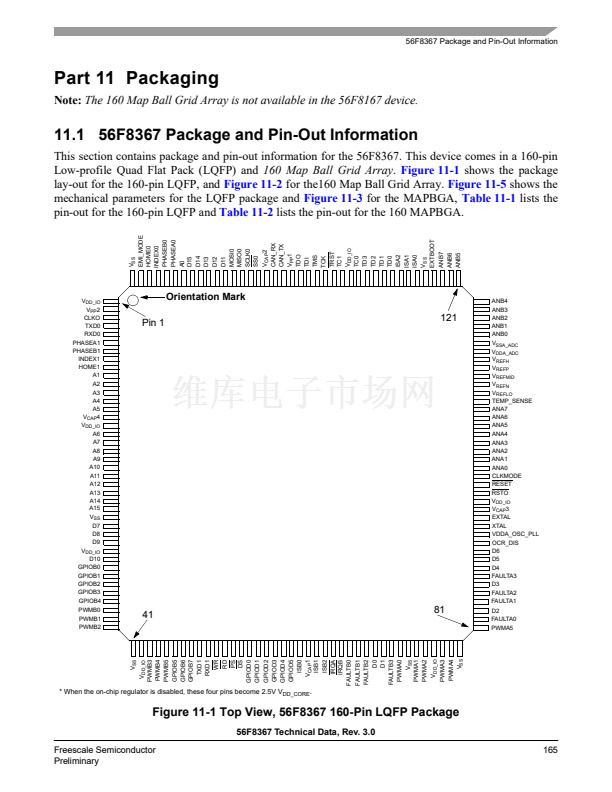
Figure 2-1 56F8367 Signals Identified by Functional Group
1
(160-pin LQFP)
1. Alternate pin functionality is shown in parenthesis; pin direction/type shown is the default functionality.
56F8367 Technical Data, Rev. 3.0
16
Freescale Semiconductor
Preliminary


 1
1
 2
2
 3
3
 4
4
 5
5
 6
6
 7
7
 8
8
 9
9
 10
10
 11
11
 12
12
 13
13
 14
14
 15
15
 16
16
 17
17
 18
18
 19
19
 20
20
 21
21
 22
22
 23
23
 24
24
 25
25
 26
26
 27
27
 28
28
 29
29
 30
30
 31
31
 32
32
 33
33
 34
34
 35
35
 36
36
 37
37
 38
38
 39
39
 40
40
 41
41
 42
42
 43
43
 44
44
 45
45
 46
46
 47
47
 48
48
 49
49
 50
50
 51
51
 52
52
 53
53
 54
54
 55
55
 56
56
 57
57
 58
58
 59
59
 60
60
 61
61
 62
62
 63
63
 64
64
 65
65
 66
66
 67
67
 68
68
 69
69
 70
70
 71
71
 72
72
 73
73
 74
74
 75
75
 76
76
 77
77
 78
78
 79
79
 80
80
 81
81
 82
82
 83
83
 84
84
 85
85
 86
86
 87
87
 88
88
 89
89
 90
90
 91
91
 92
92
 93
93
 94
94
 95
95
 96
96
 97
97
 98
98
 99
99
 100
100
 101
101
 102
102
 103
103
 104
104
 105
105
 106
106
 107
107
 108
108
 109
109
 110
110
 111
111
 112
112
 113
113
 114
114
 115
115
 116
116
 117
117
 118
118
 119
119
 120
120
 121
121
 122
122
 123
123
 124
124
 125
125
 126
126
 127
127
 128
128
 129
129
 130
130
 131
131
 132
132
 133
133
 134
134
 135
135
 136
136
 137
137
 138
138
 139
139
 140
140
 141
141
 142
142
 143
143
 144
144
 145
145
 146
146
 147
147
 148
148
 149
149
 150
150
 151
151
 152
152
 153
153
 154
154
 155
155
 156
156
 157
157
 158
158
 159
159
 160
160
 161
161
 162
162
 163
163
 164
164
 165
165
 166
166
 167
167
 168
168
 169
169
 170
170
 171
171
 172
172
 173
173
 174
174
 175
175
 176
176
 177
177
 178
178
 179
179
 180
180
