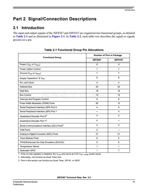
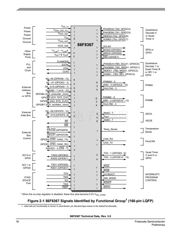
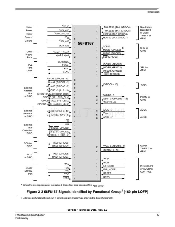
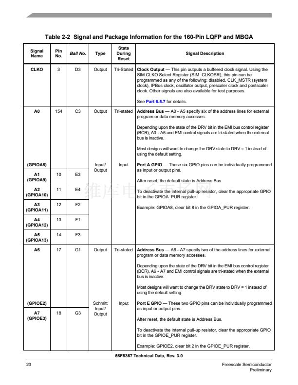
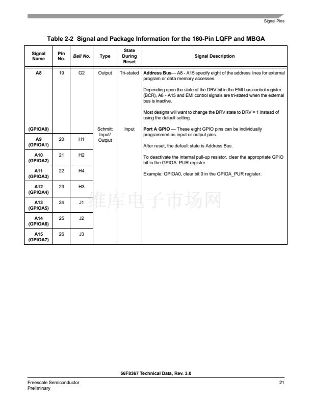
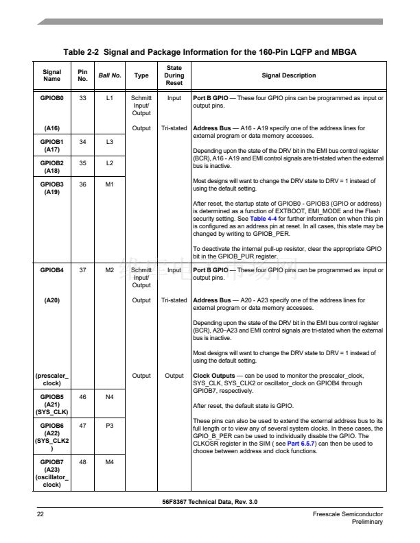
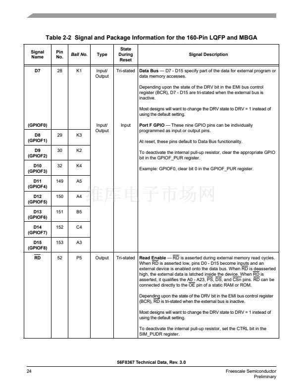
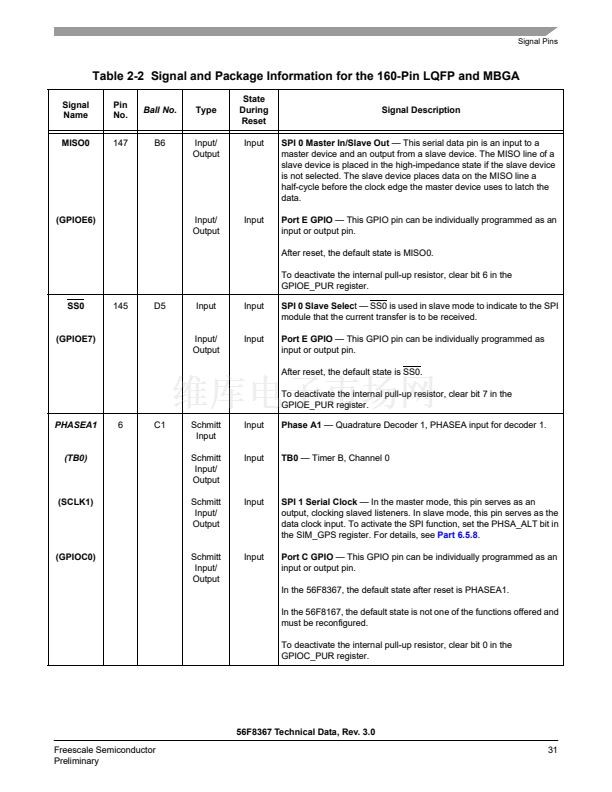
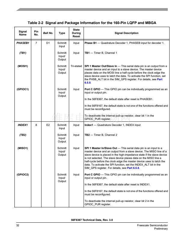
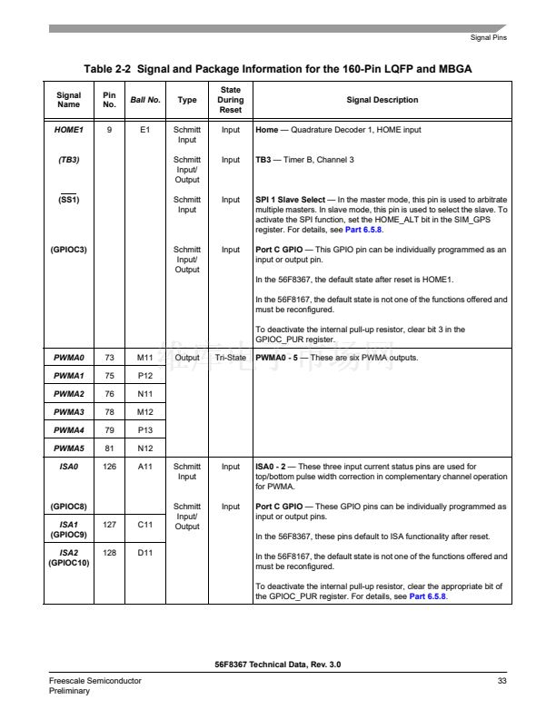
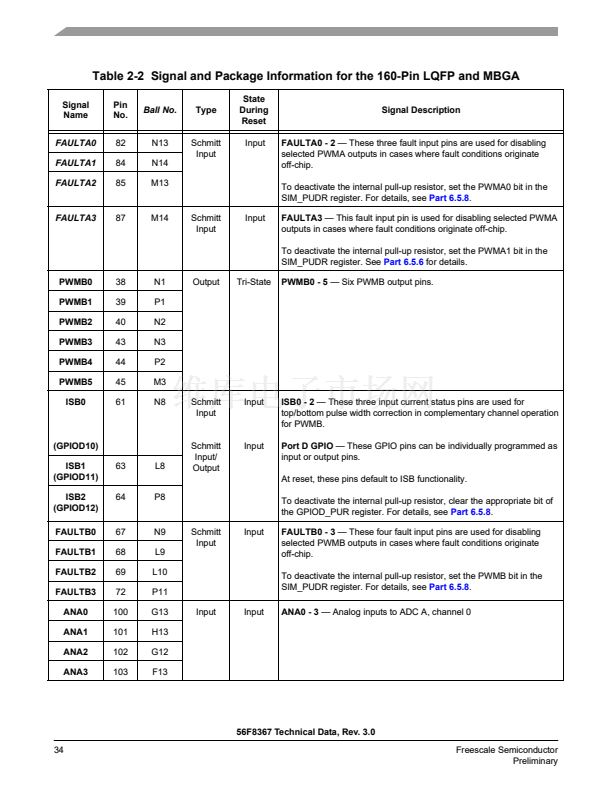
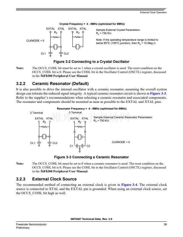
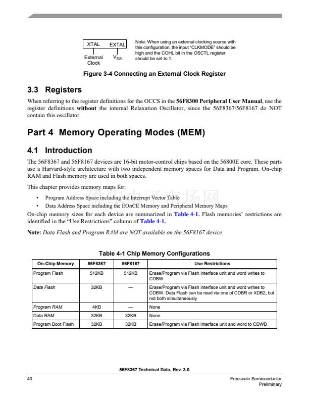
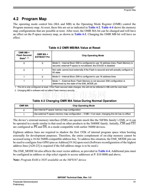
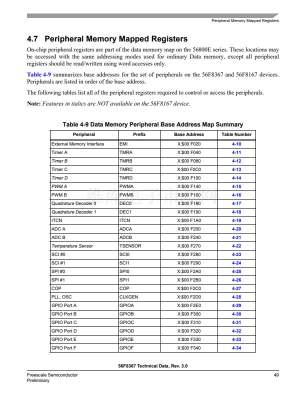
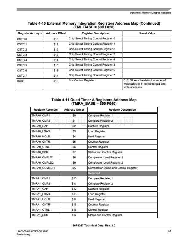
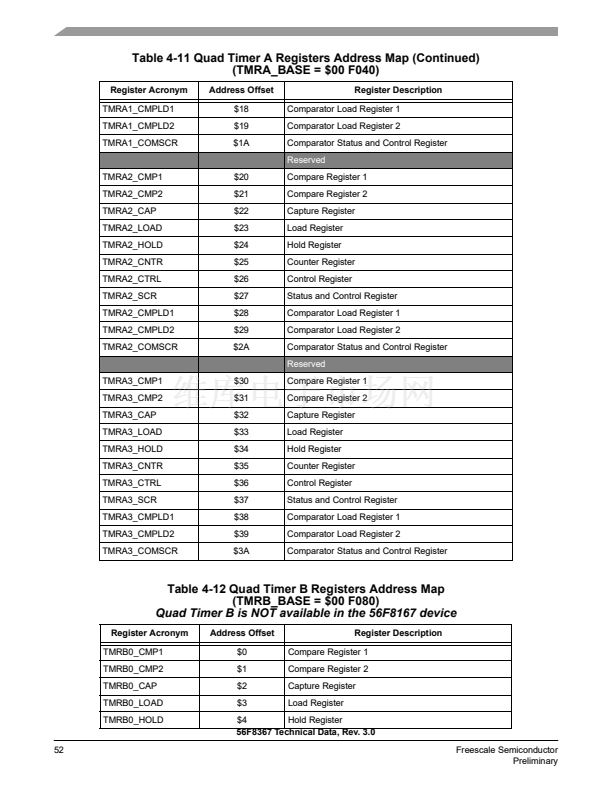
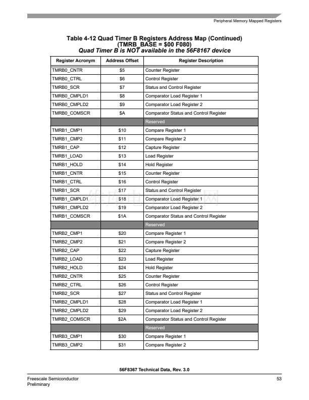
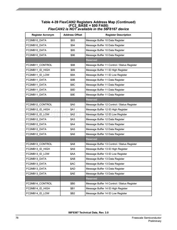
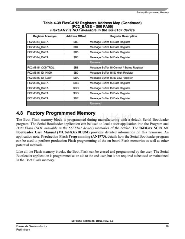
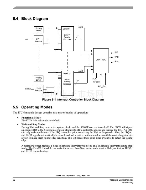
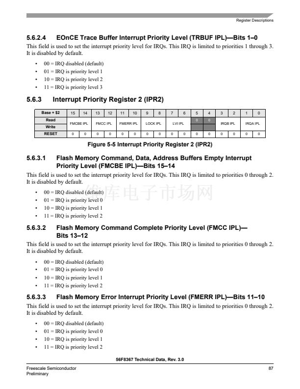
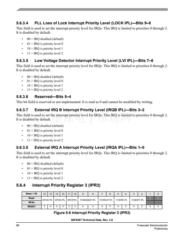
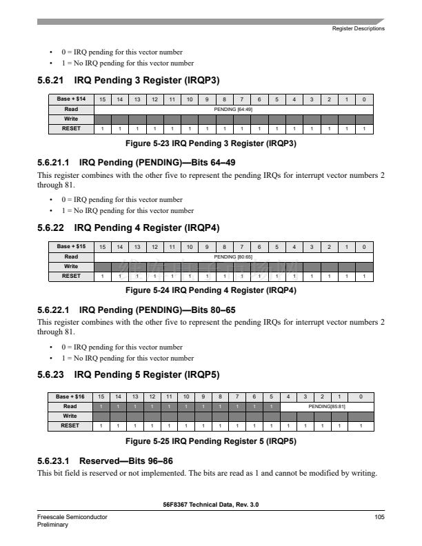
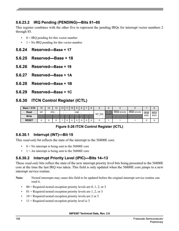
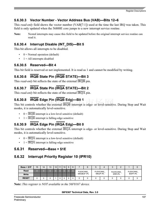
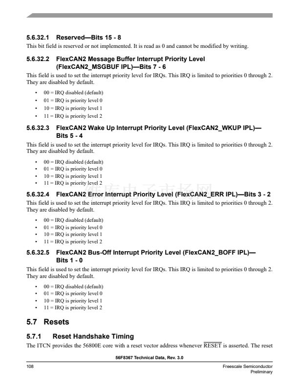
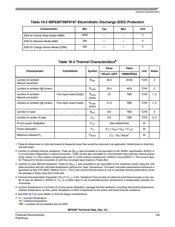
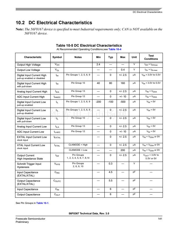
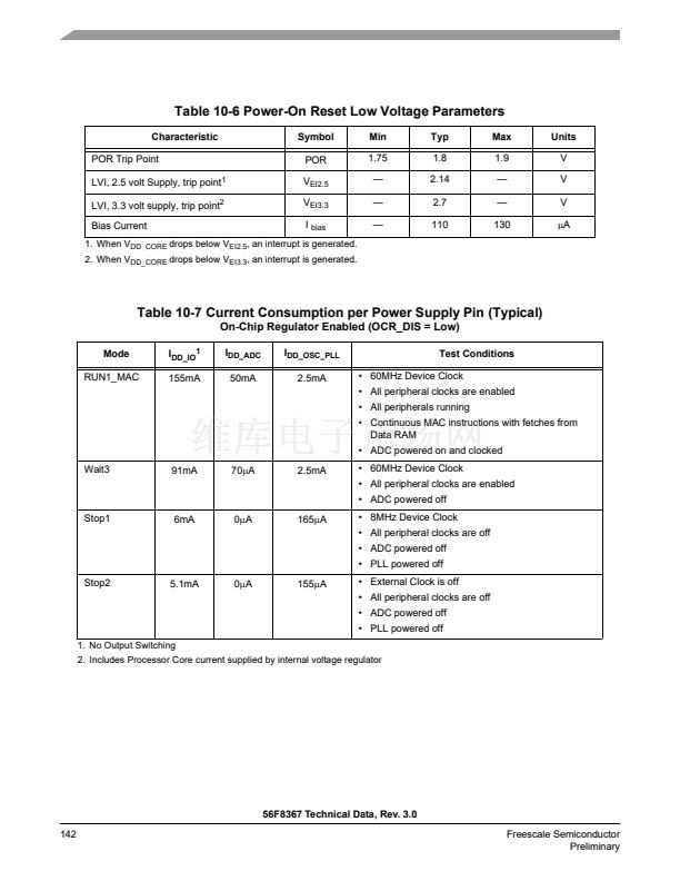
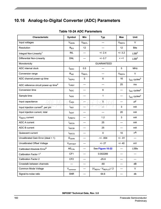
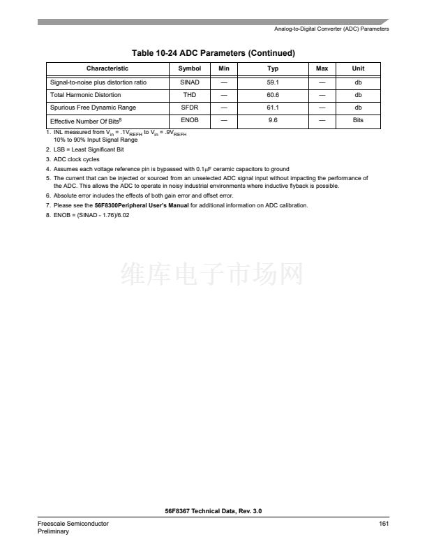
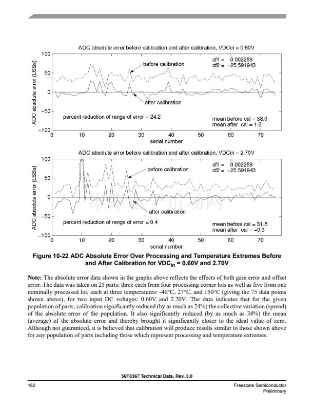
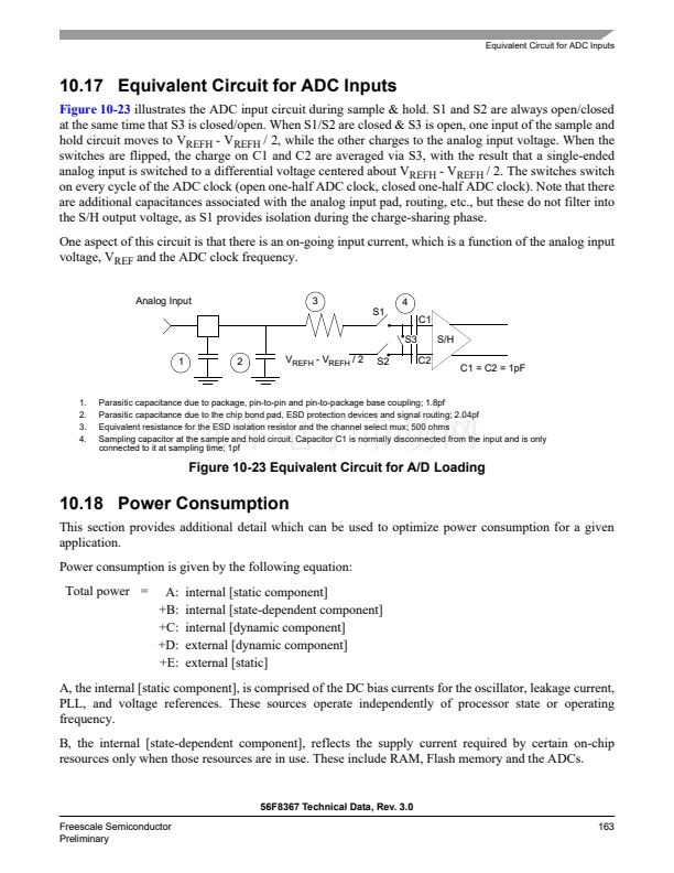
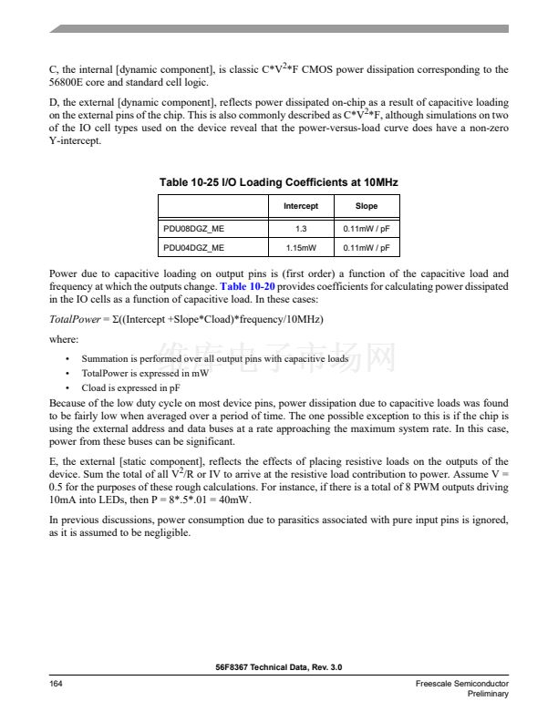
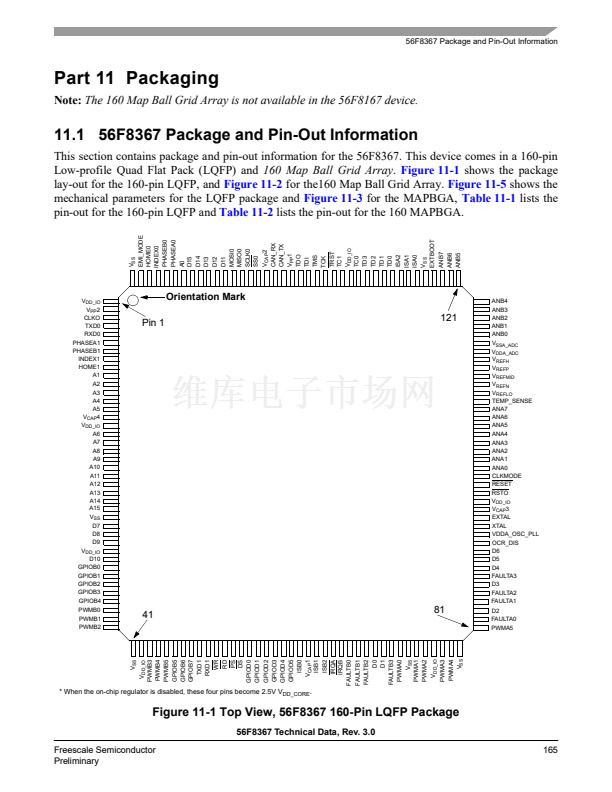
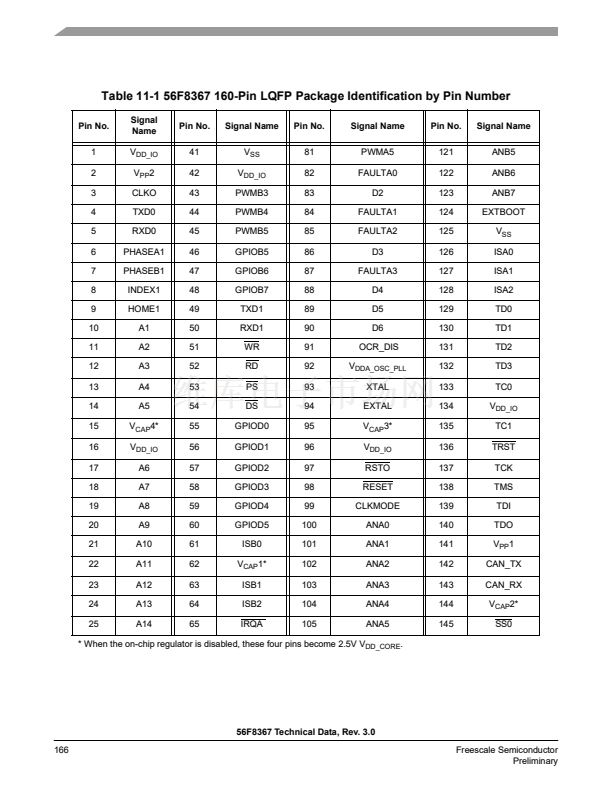
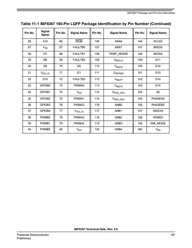
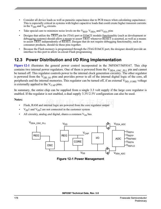
Signal Pins
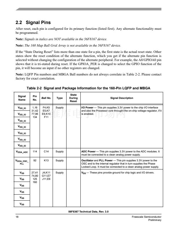
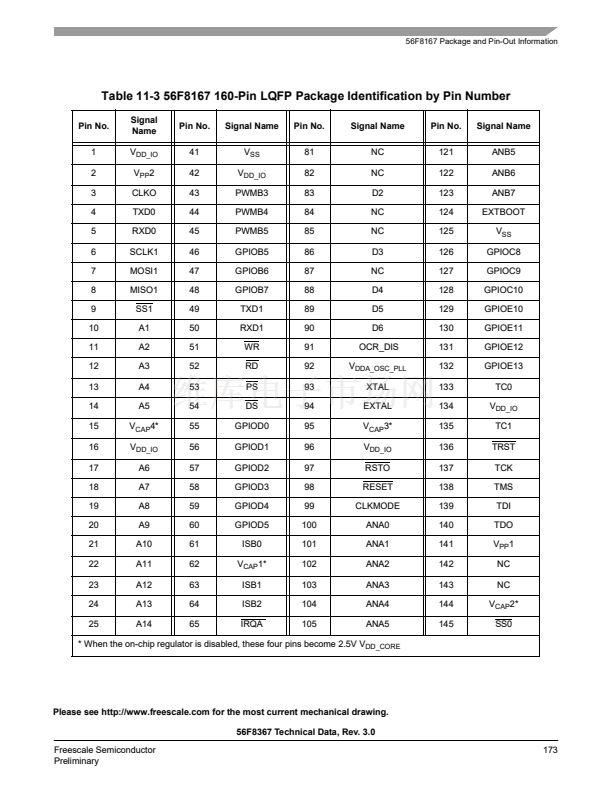
Table 2-2 Signal and Package Information for the 160-Pin LQFP and MBGA
Signal
Name
ANA4
ANA5
ANA6
ANA7
V
REFH
Pin
No.
104
105
106
107
113
Ball No.
Type
State
During
Reset
Input
Signal Description
F12
H14
G14
E13
D14
Input
ANA4 - 7
鈥?Analog inputs to ADC A, channel 1
Input
Input
V
REFH
鈥?Analog Reference Voltage High. V
REFH
must be less than or
equal to V
DDA_ADC.
V
REFP
, V
REFMID
& V
REFN
鈥?Internal pins for voltage reference which
are brought off-chip so they can be bypassed. Connect to a 0.1碌F low
ESR capacitor.
V
REFP
V
REFMID
V
REFN
V
REFLO
112
111
110
109
D13
E14
F14
E12
Input/
Output
Input/
Output
Input
Input
V
REFLO
鈥?Analog Reference Voltage Low. This should normally be
connected to a low-noise V
SS
.
ANB0 - 3
鈥?Analog inputs to ADC B, channel 0
ANB0
ANB1
ANB2
ANB3
ANB4
ANB5
ANB6
ANB7
TEMP_SEN
SE
116
117
118
119
120
121
122
123
108
C13
B14
C12
B13
A14
A13
B12
A12
E11
Input
Input
Input
Input
ANB4 - 7
鈥?Analog inputs to ADC B, channel 1
Output
Output
Temperature Sense Diode
鈥?This signal connects to an on-chip
diode that can be connected to one of the ADC inputs and used to
monitor the temperature of the die. Must be bypassed with a 0.01碌F
capacitor.
FlexCAN Receive Data
鈥?This is the CAN input. This pin has an
internal pull-up resistor.
To deactivate the internal pull-up resistor, set the CAN bit in the
SIM_PUDR register.
CAN_RX
143
B7
Schmitt
Input
Input
CAN_TX
142
D6
Open
Drain
Output
Open
Drain
Output
FlexCAN Transmit Data
鈥?CAN output
56F8367 Technical Data, Rev. 3.0
Freescale Semiconductor
Preliminary
35


 1
1
 2
2
 3
3
 4
4
 5
5
 6
6
 7
7
 8
8
 9
9
 10
10
 11
11
 12
12
 13
13
 14
14
 15
15
 16
16
 17
17
 18
18
 19
19
 20
20
 21
21
 22
22
 23
23
 24
24
 25
25
 26
26
 27
27
 28
28
 29
29
 30
30
 31
31
 32
32
 33
33
 34
34
 35
35
 36
36
 37
37
 38
38
 39
39
 40
40
 41
41
 42
42
 43
43
 44
44
 45
45
 46
46
 47
47
 48
48
 49
49
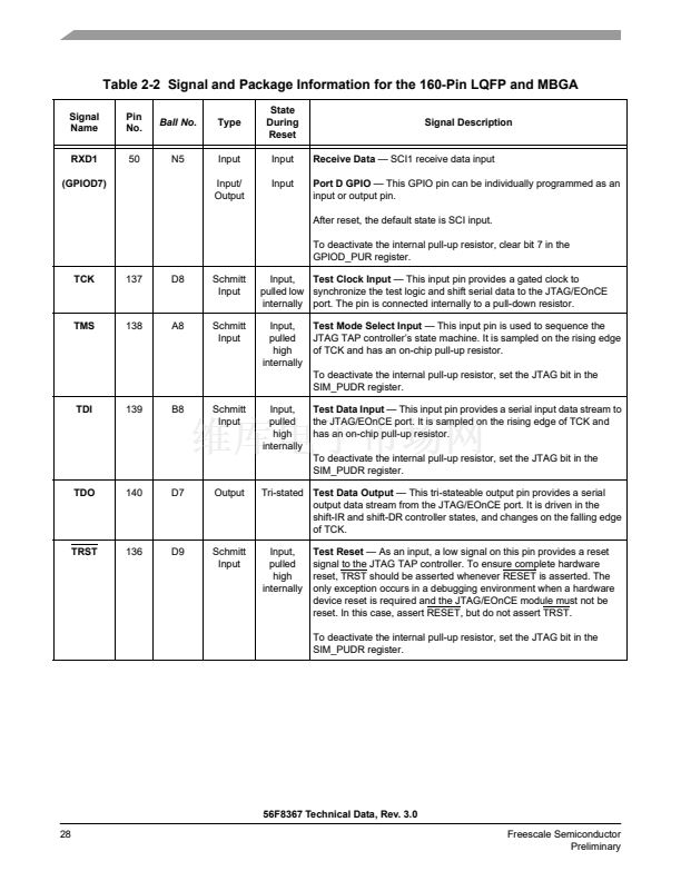
 50
50
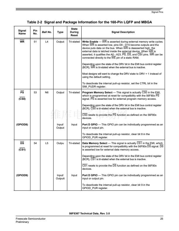
 51
51
 52
52
 53
53
 54
54
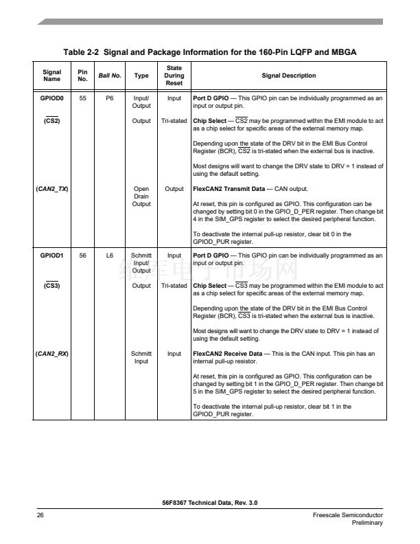
 55
55
 56
56
 57
57
 58
58
 59
59
 60
60
 61
61
 62
62
 63
63
 64
64
 65
65
 66
66
 67
67
 68
68
 69
69
 70
70
 71
71
 72
72
 73
73
 74
74
 75
75
 76
76
 77
77
 78
78
 79
79
 80
80
 81
81
 82
82
 83
83
 84
84
 85
85
 86
86
 87
87
 88
88
 89
89
 90
90
 91
91
 92
92
 93
93
 94
94
 95
95
 96
96
 97
97
 98
98
 99
99
 100
100
 101
101
 102
102
 103
103
 104
104
 105
105
 106
106
 107
107
 108
108
 109
109
 110
110
 111
111
 112
112
 113
113
 114
114
 115
115
 116
116
 117
117
 118
118
 119
119
 120
120
 121
121
 122
122
 123
123
 124
124
 125
125
 126
126
 127
127
 128
128
 129
129
 130
130
 131
131
 132
132
 133
133
 134
134
 135
135
 136
136
 137
137
 138
138
 139
139
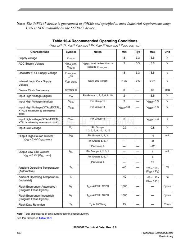 140
140
 141
141
 142
142
 143
143
 144
144
 145
145
 146
146
 147
147
 148
148
 149
149
 150
150
 151
151
 152
152
 153
153
 154
154
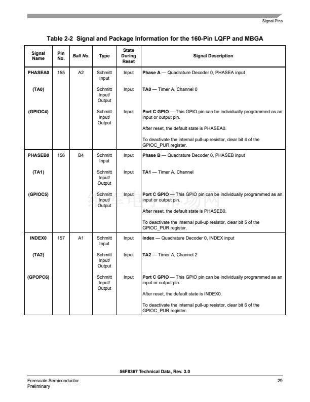
 155
155
 156
156
 157
157
 158
158
 159
159
 160
160
 161
161
 162
162
 163
163
 164
164
 165
165
 166
166
 167
167
 168
168
 169
169
 170
170
 171
171
 172
172
 173
173
 174
174
 175
175
 176
176
 177
177
 178
178
 179
179
 180
180
