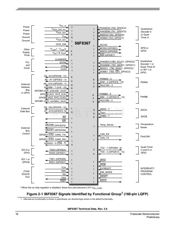
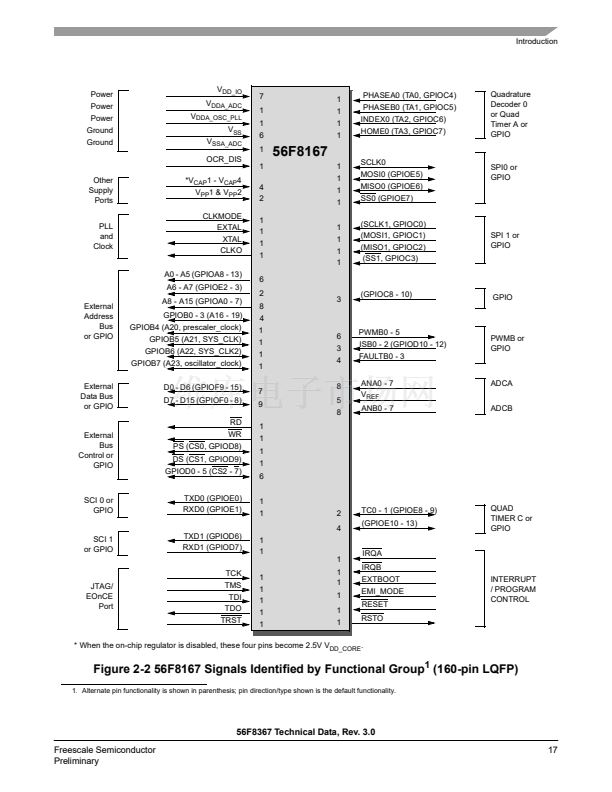
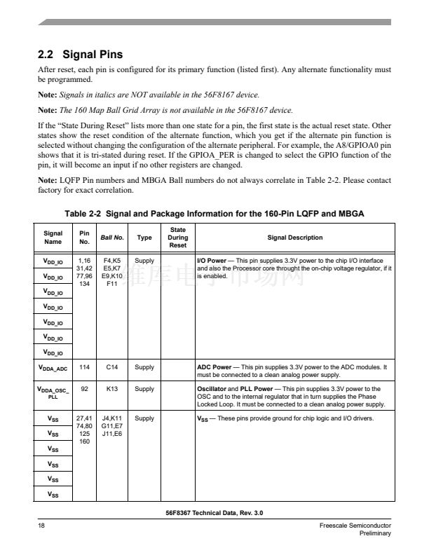
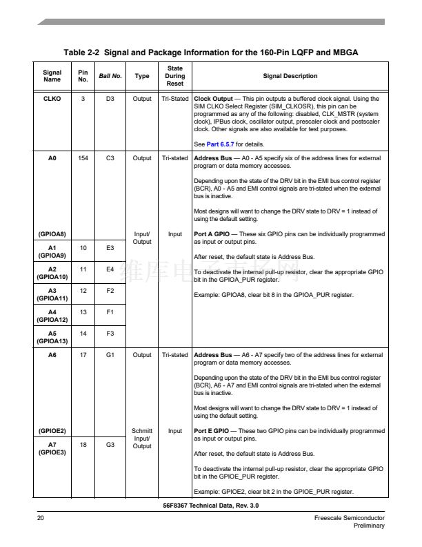
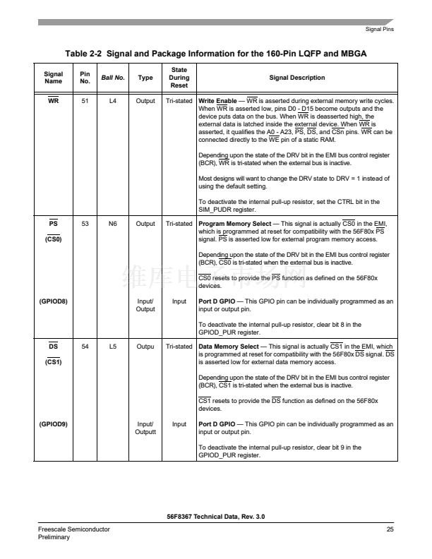
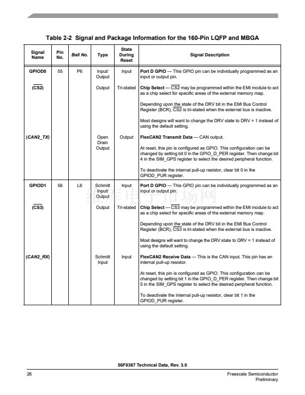
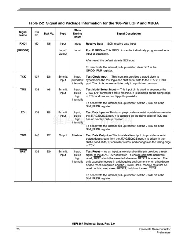
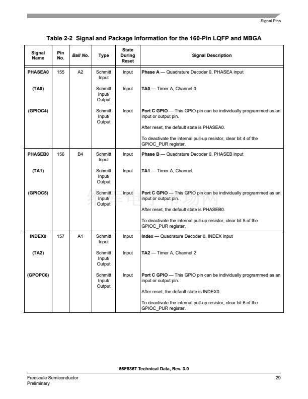
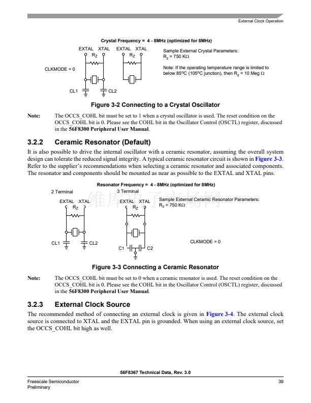
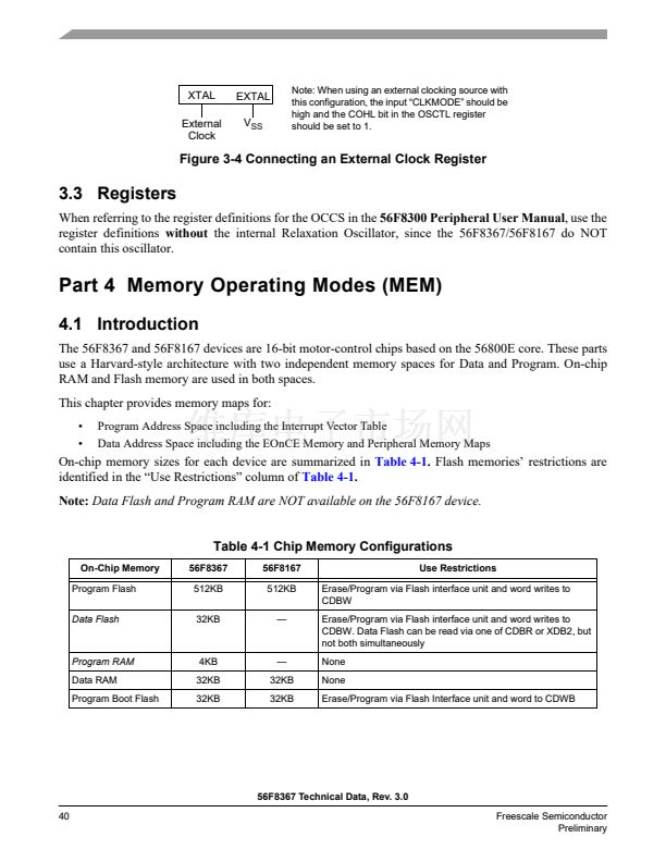
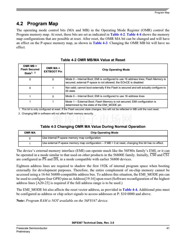
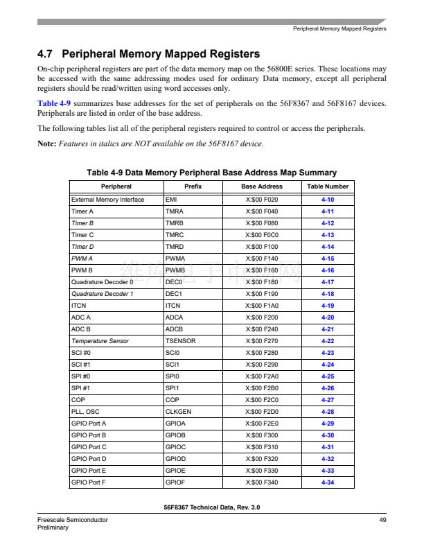
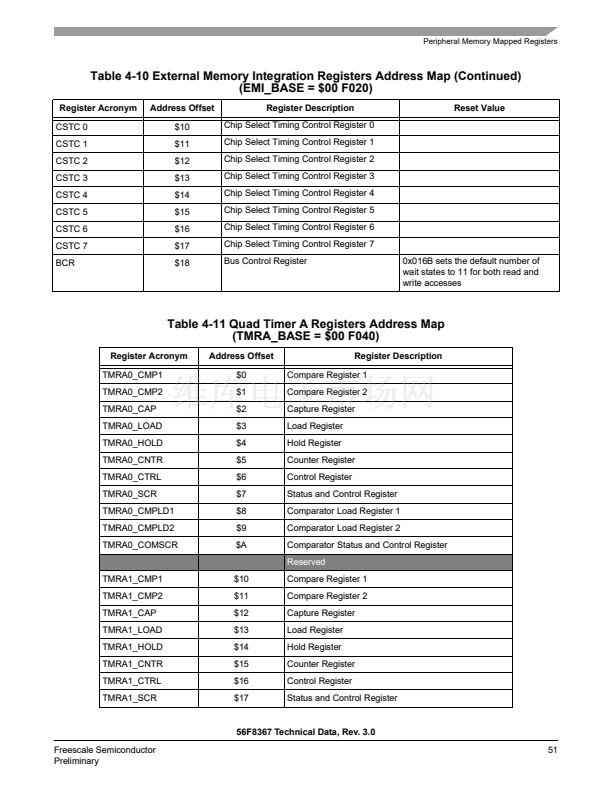
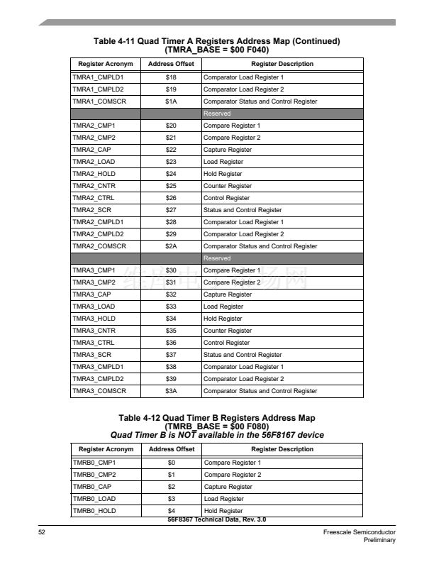
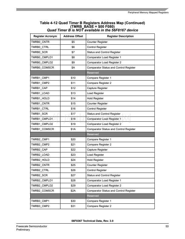
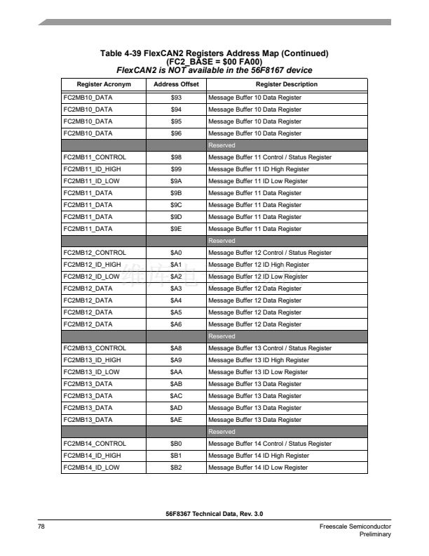
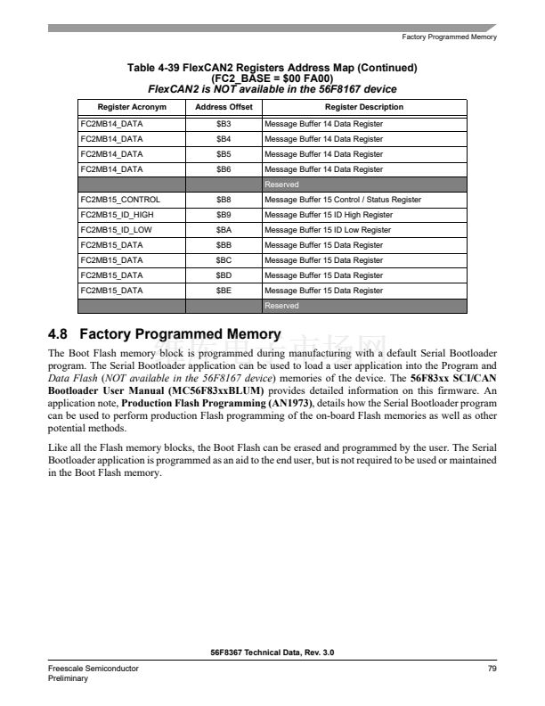
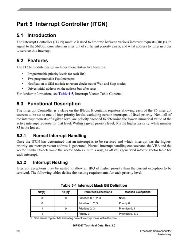
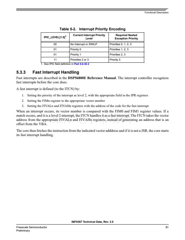
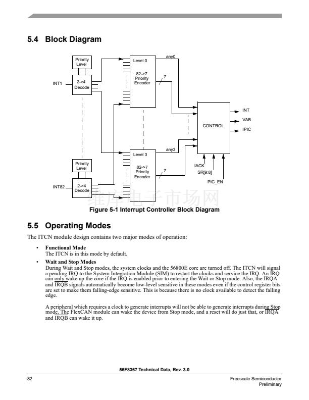
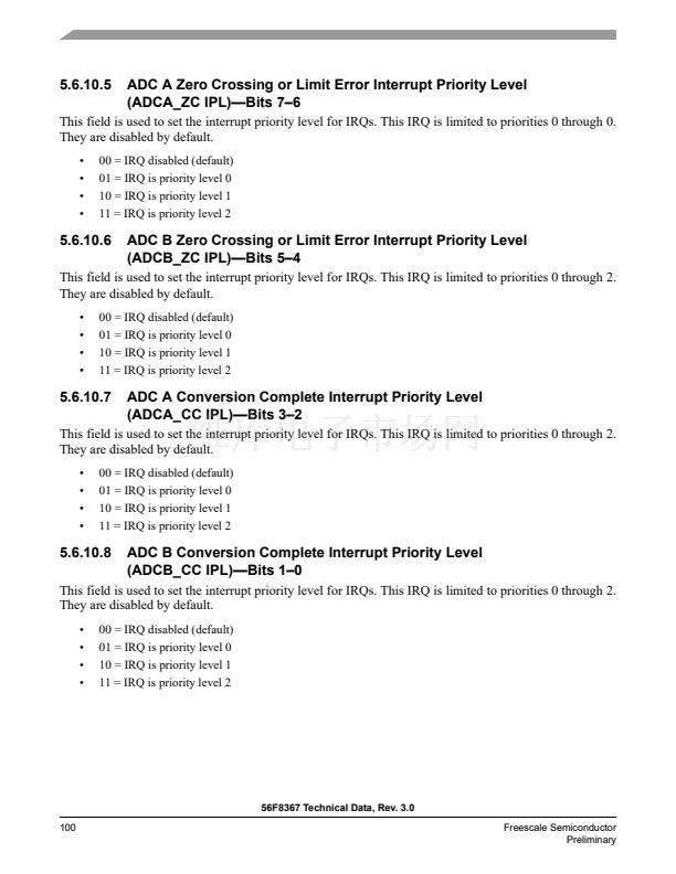
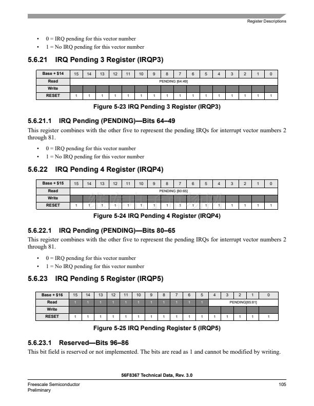
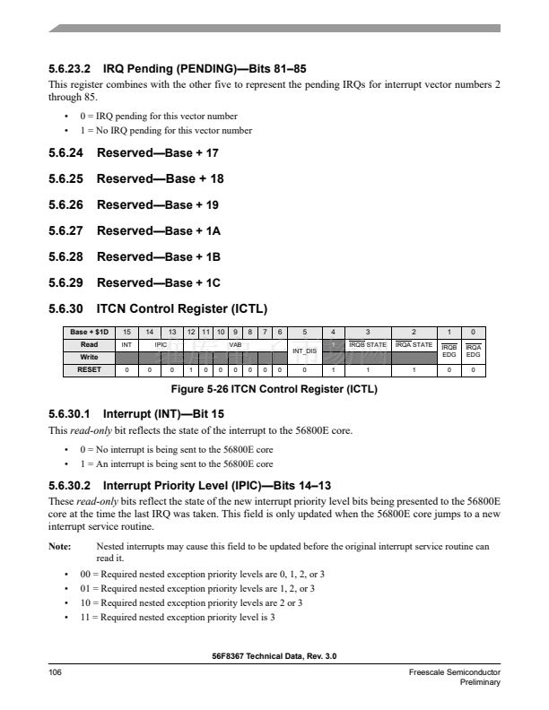
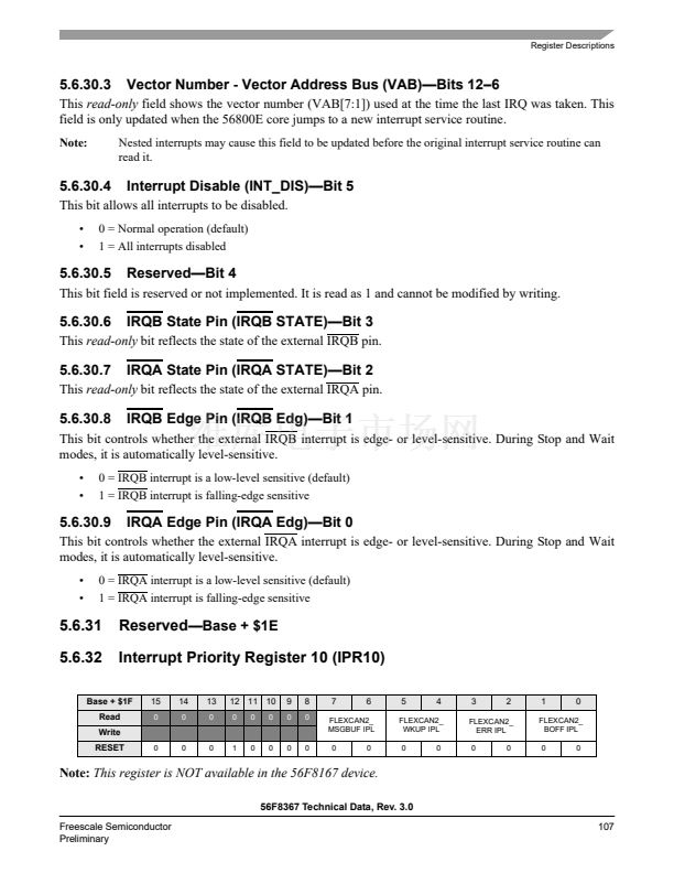
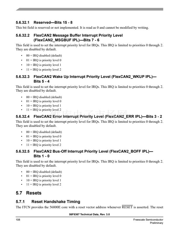
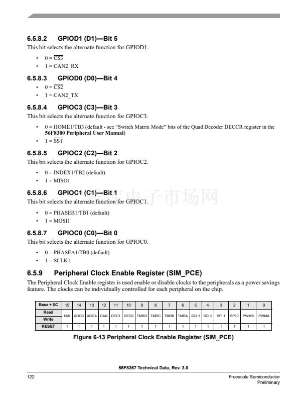
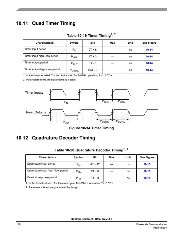
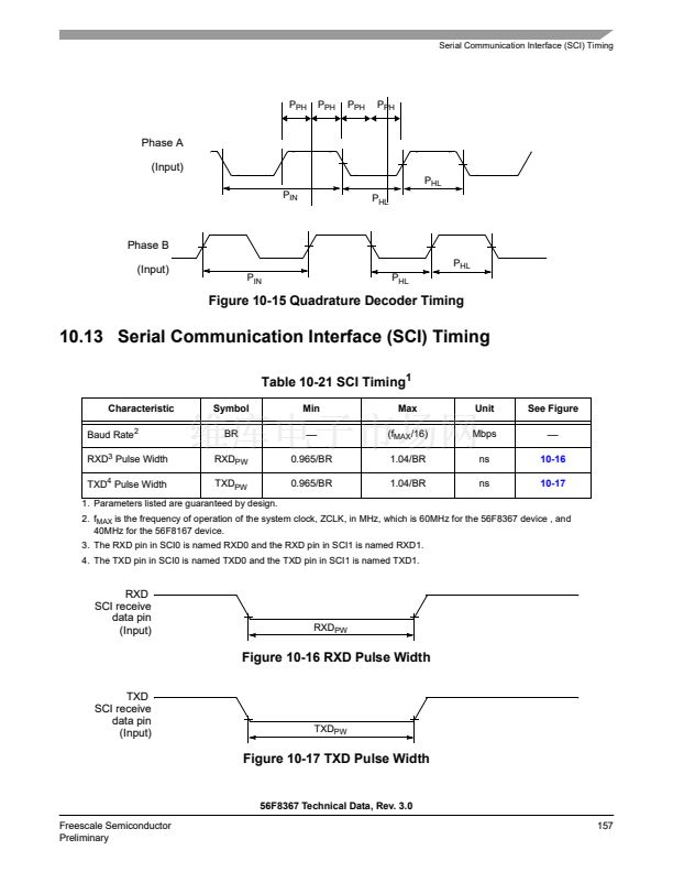
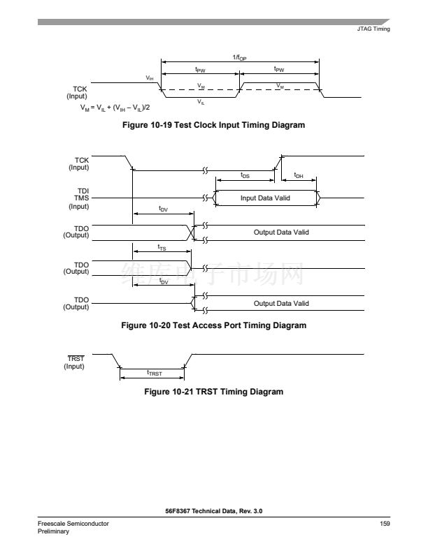
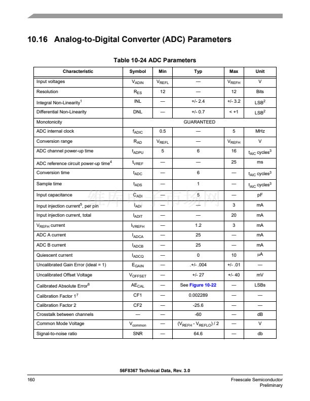
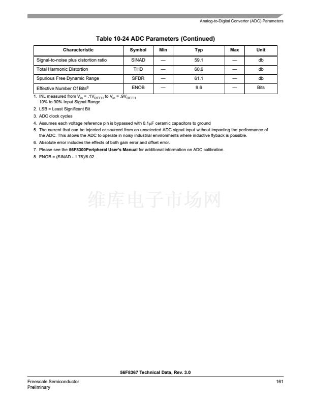
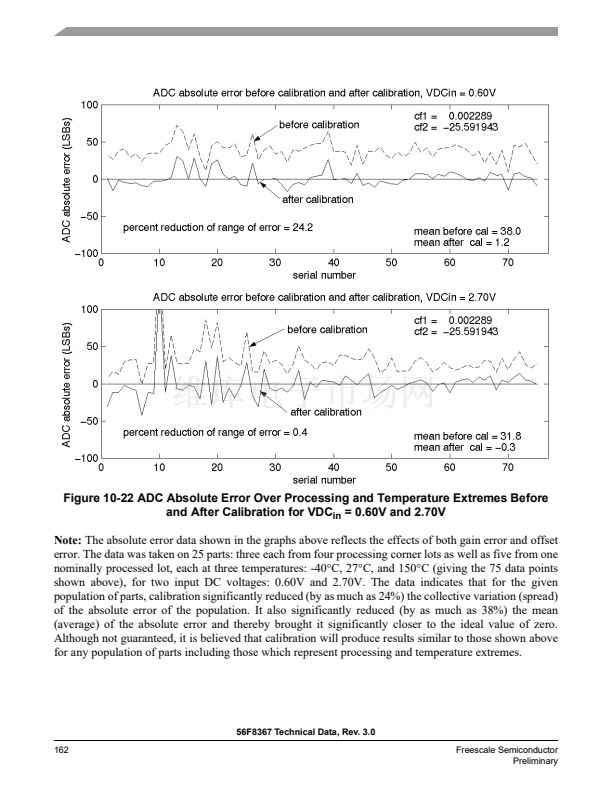
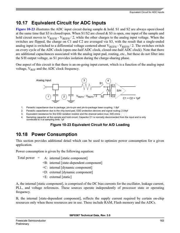
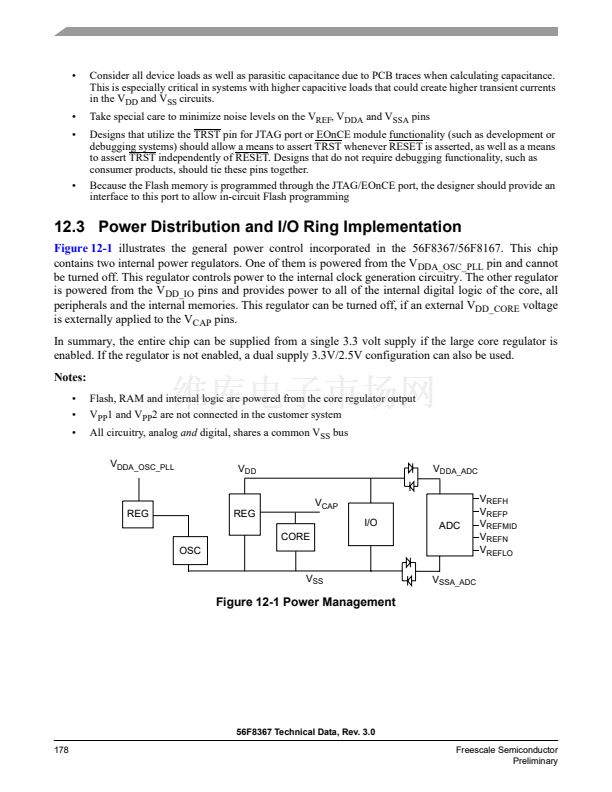
2.2 Signal Pins
After reset, each pin is configured for its primary function (listed first). Any alternate functionality must
be programmed.
Note:
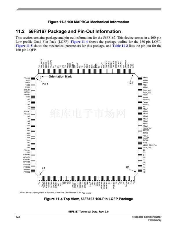
Signals in italics are NOT available in the 56F8167 device.
Note:
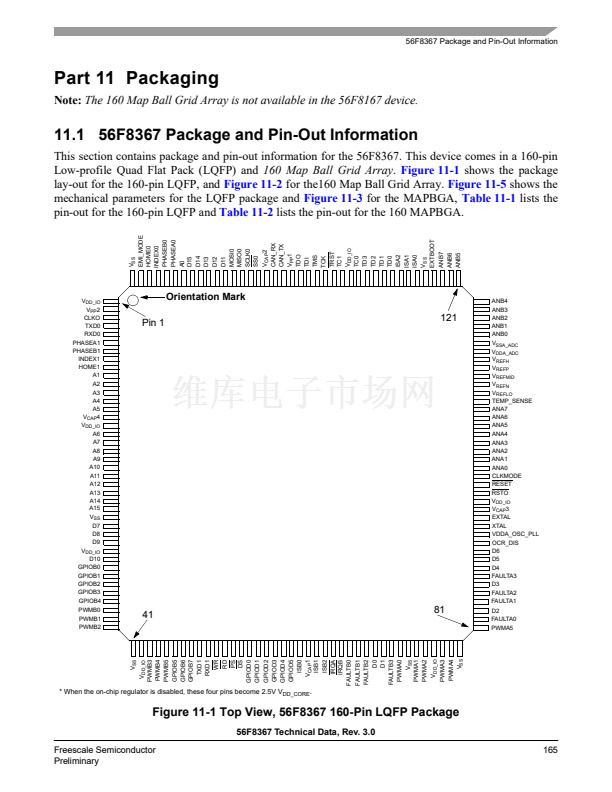
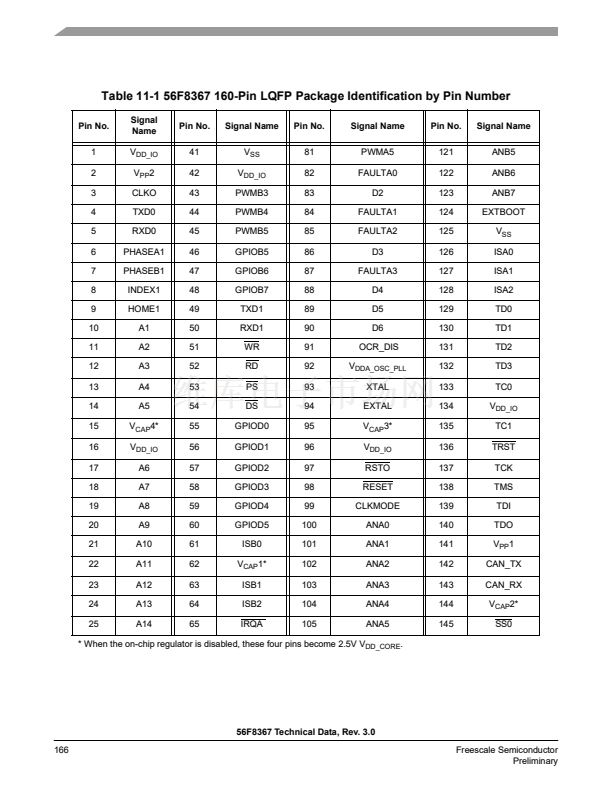
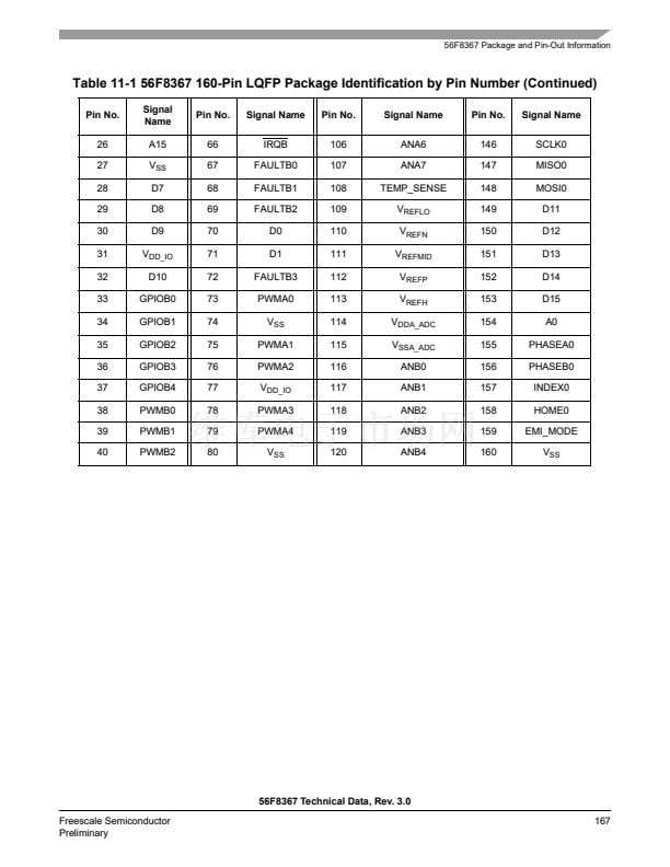
The 160 Map Ball Grid Array is not available in the 56F8167 device.
If the 鈥淪tate During Reset鈥?lists more than one state for a pin, the first state is the actual reset state. Other
states show the reset condition of the alternate function, which you get if the alternate pin function is
selected without changing the configuration of the alternate peripheral. For example, the A8/GPIOA0 pin
shows that it is tri-stated during reset. If the GPIOA_PER is changed to select the GPIO function of the
pin, it will become an input if no other registers are changed.
Note:
LQFP Pin numbers and MBGA Ball numbers do not always correlate in Table 2-2. Please contact
factory for exact correlation.
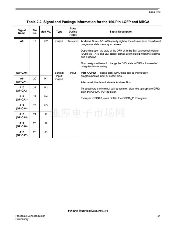
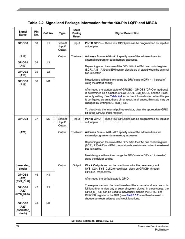
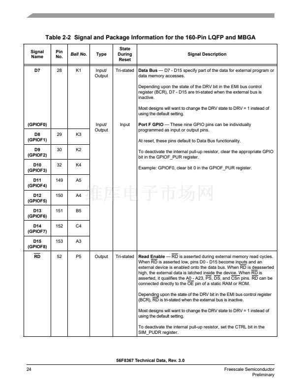
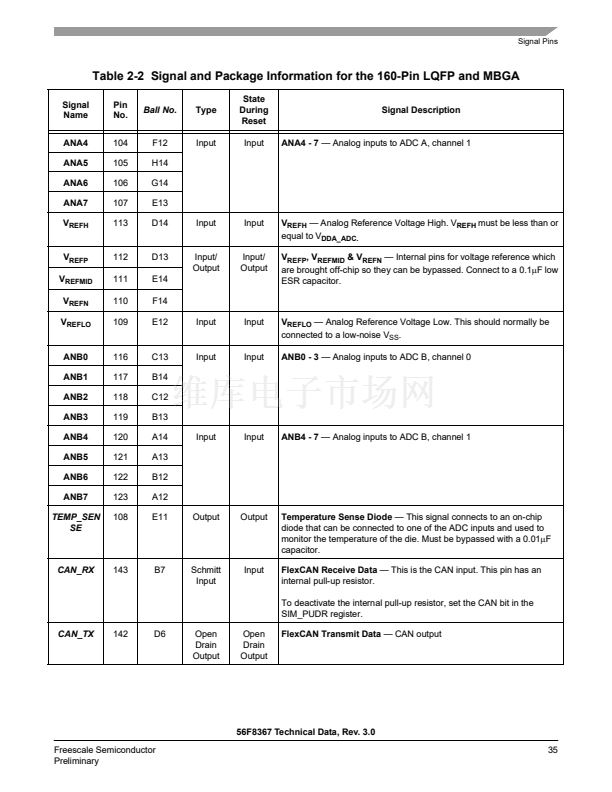
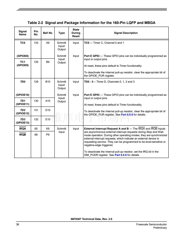
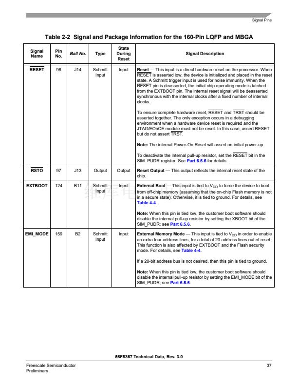
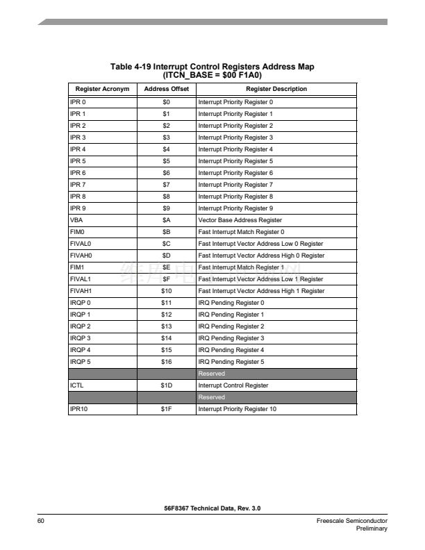
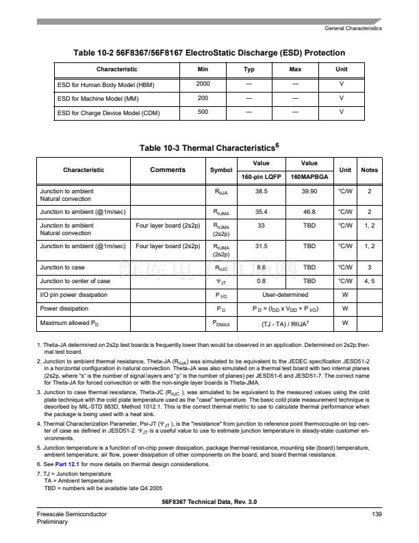
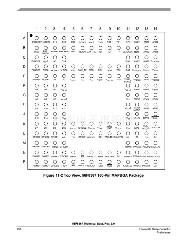
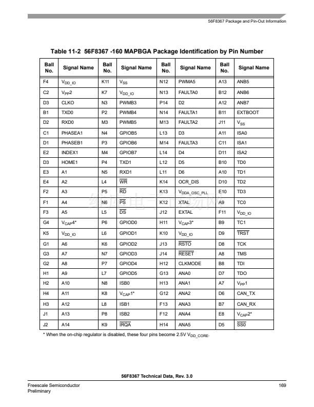
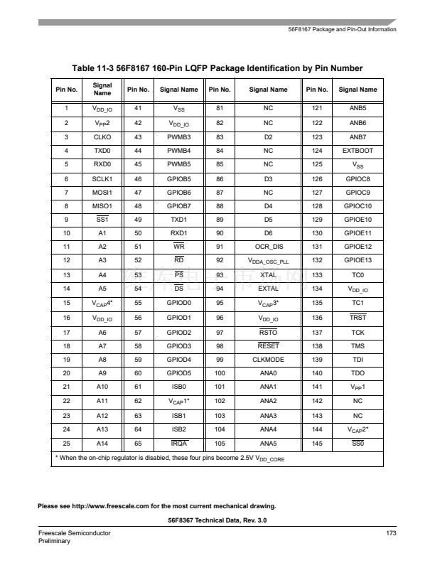
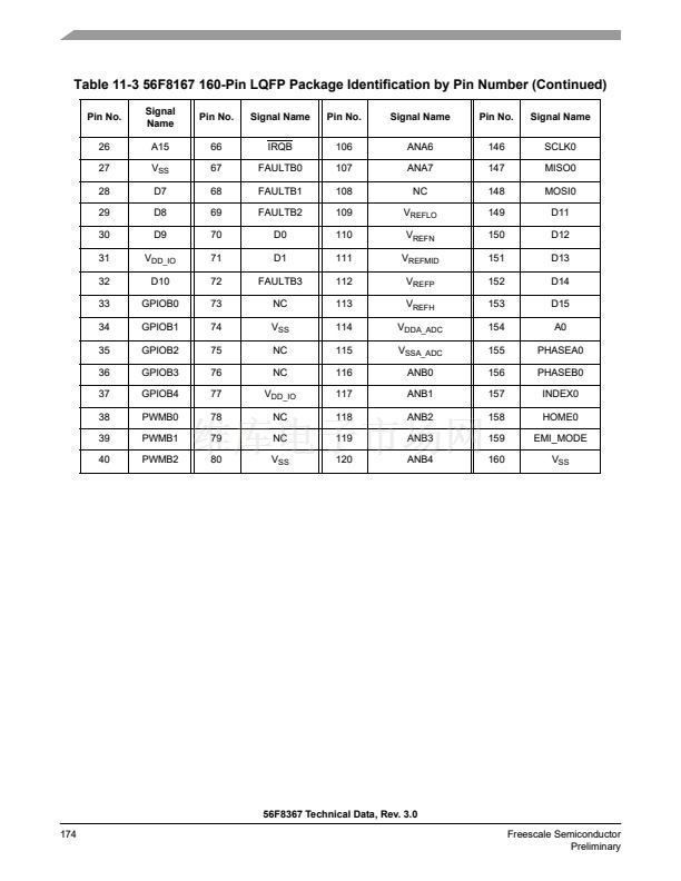
Table 2-2 Signal and Package Information for the 160-Pin LQFP and MBGA
Signal
Name
V
DD_IO
V
DD_IO
V
DD_IO
V
DD_IO
V
DD_IO
V
DD_IO
V
DD_IO
V
DDA_ADC
V
DDA_OSC_
PLL
Pin
No.
1,16
31,42
77,96
134
Ball No.
Type
State
During
Reset
Signal Description
F4,K5
E5,K7
E9,K10
F11
Supply
I/O Power
鈥?This pin supplies 3.3V power to the chip I/O interface
and also the Processor core throught the on-chip voltage regulator, if it
is enabled.
114
C14
Supply
ADC Power
鈥?This pin supplies 3.3V power to the ADC modules. It
must be connected to a clean analog power supply.
Oscillator
and
PLL Power
鈥?This pin supplies 3.3V power to the
OSC and to the internal regulator that in turn supplies the Phase
Locked Loop. It must be connected to a clean analog power supply.
V
SS
鈥?These pins provide ground for chip logic and I/O drivers.
92
K13
Supply
V
SS
V
SS
V
SS
V
SS
V
SS
V
SS
27,41
74,80
125
160
J4,K11
G11,E7
J11,E6
Supply
56F8367 Technical Data, Rev. 3.0
18
Freescale Semiconductor
Preliminary


 1
1
 2
2
 3
3
 4
4
 5
5
 6
6
 7
7
 8
8
 9
9
 10
10
 11
11
 12
12
 13
13
 14
14
 15
15
 16
16
 17
17
 18
18
 19
19
 20
20
 21
21
 22
22
 23
23
 24
24
 25
25
 26
26
 27
27
 28
28
 29
29
 30
30
 31
31
 32
32
 33
33
 34
34
 35
35
 36
36
 37
37
 38
38
 39
39
 40
40
 41
41
 42
42
 43
43
 44
44
 45
45
 46
46
 47
47
 48
48
 49
49
 50
50
 51
51
 52
52
 53
53
 54
54
 55
55
 56
56
 57
57
 58
58
 59
59
 60
60
 61
61
 62
62
 63
63
 64
64
 65
65
 66
66
 67
67
 68
68
 69
69
 70
70
 71
71
 72
72
 73
73
 74
74
 75
75
 76
76
 77
77
 78
78
 79
79
 80
80
 81
81
 82
82
 83
83
 84
84
 85
85
 86
86
 87
87
 88
88
 89
89
 90
90
 91
91
 92
92
 93
93
 94
94
 95
95
 96
96
 97
97
 98
98
 99
99
 100
100
 101
101
 102
102
 103
103
 104
104
 105
105
 106
106
 107
107
 108
108
 109
109
 110
110
 111
111
 112
112
 113
113
 114
114
 115
115
 116
116
 117
117
 118
118
 119
119
 120
120
 121
121
 122
122
 123
123
 124
124
 125
125
 126
126
 127
127
 128
128
 129
129
 130
130
 131
131
 132
132
 133
133
 134
134
 135
135
 136
136
 137
137
 138
138
 139
139
 140
140
 141
141
 142
142
 143
143
 144
144
 145
145
 146
146
 147
147
 148
148
 149
149
 150
150
 151
151
 152
152
 153
153
 154
154
 155
155
 156
156
 157
157
 158
158
 159
159
 160
160
 161
161
 162
162
 163
163
 164
164
 165
165
 166
166
 167
167
 168
168
 169
169
 170
170
 171
171
 172
172
 173
173
 174
174
 175
175
 176
176
 177
177
 178
178
 179
179
 180
180
