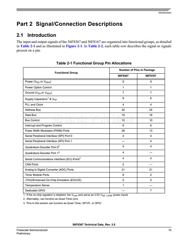
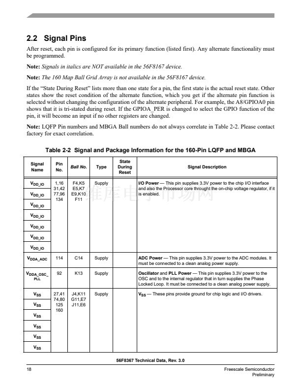
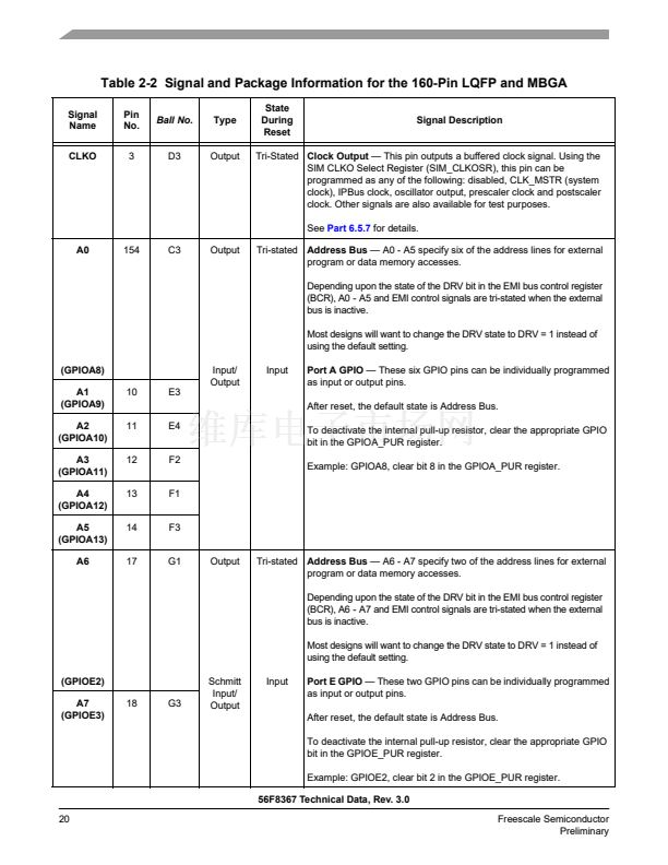
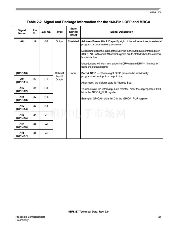
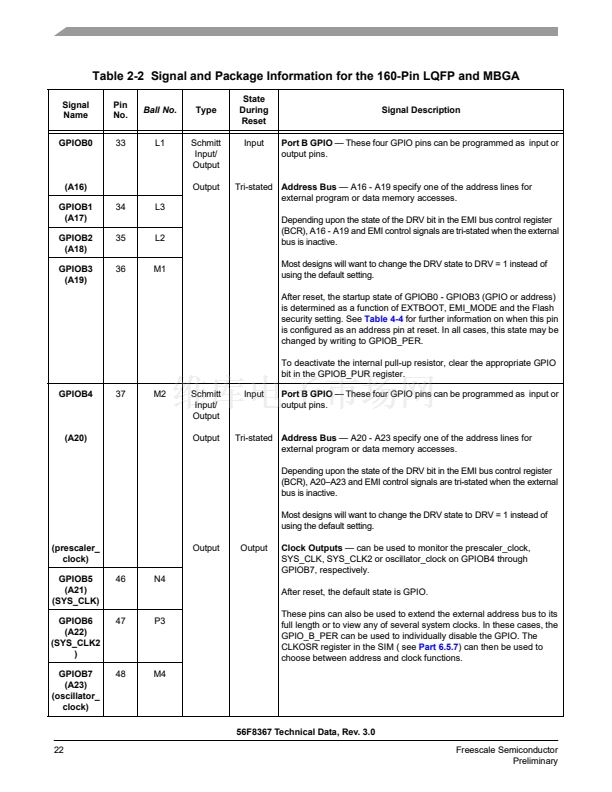
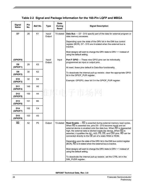
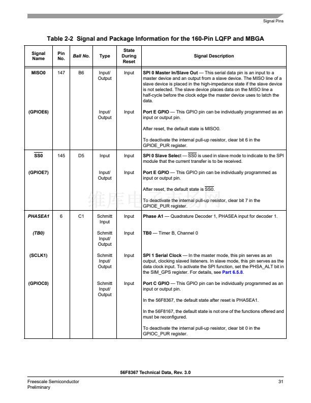
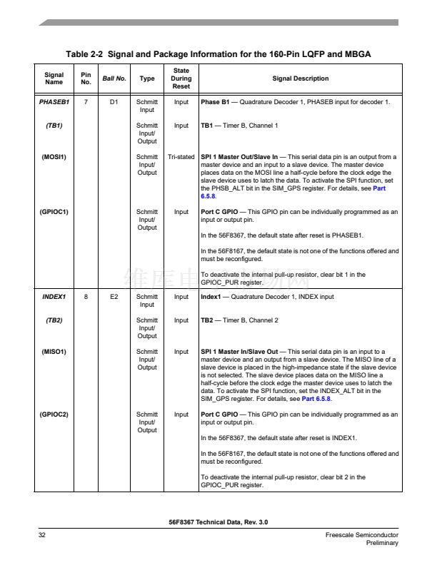
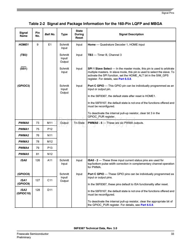
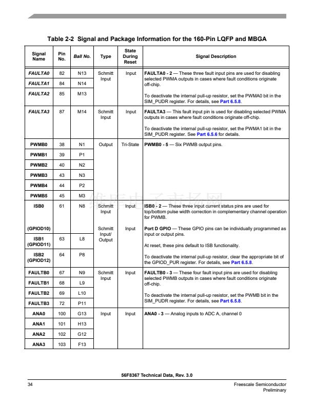
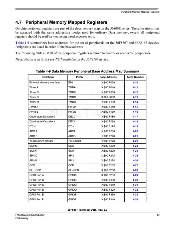
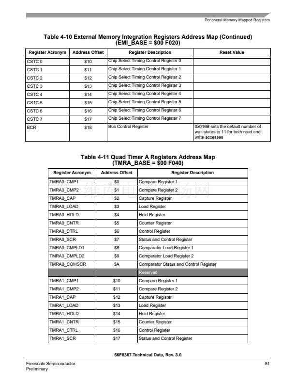
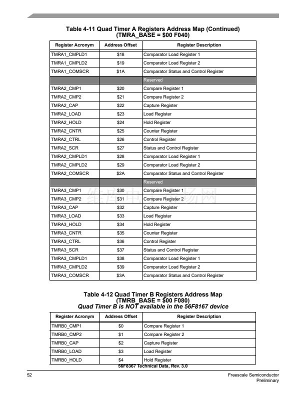
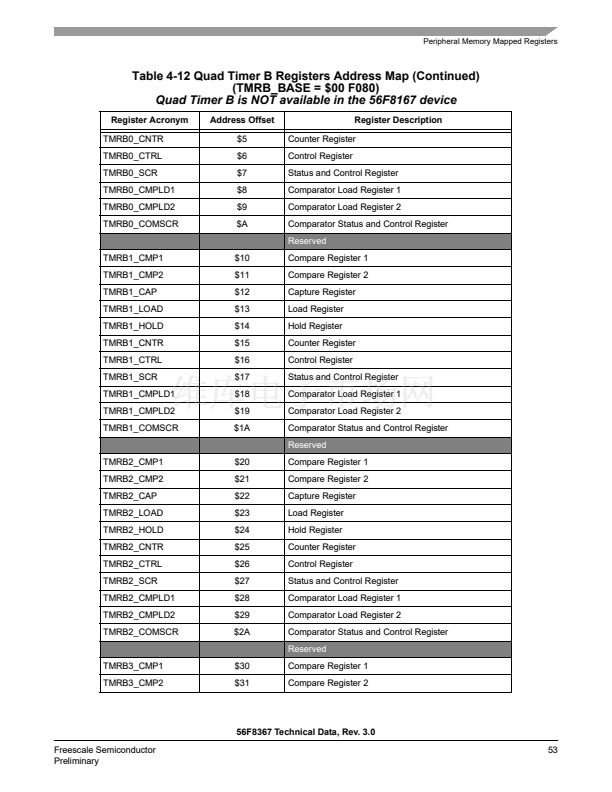
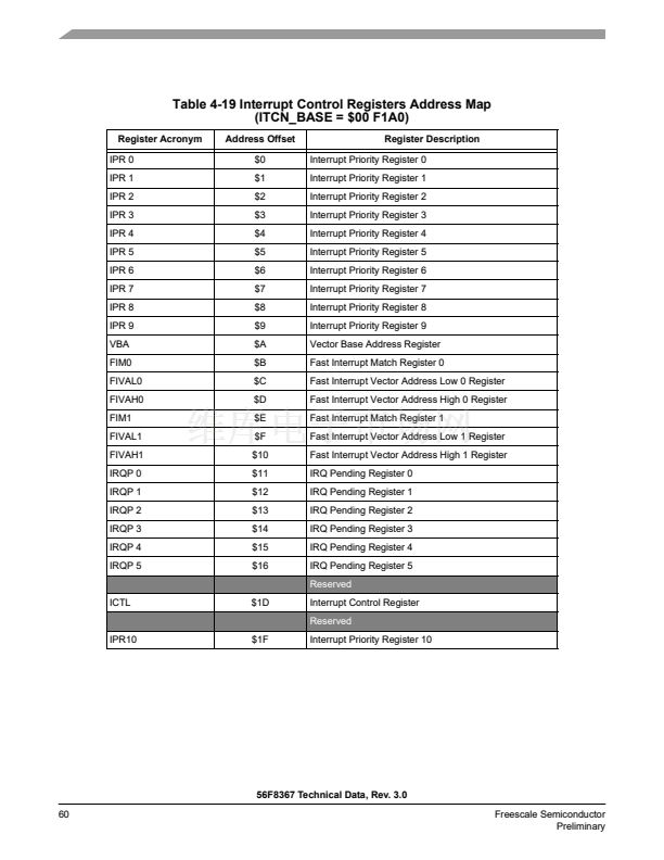
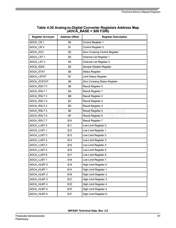
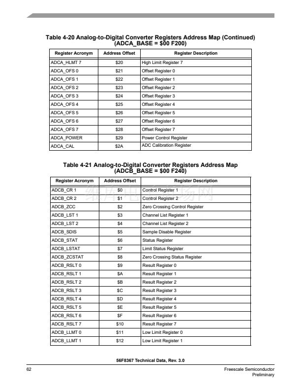
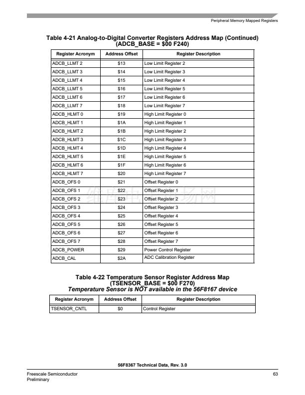
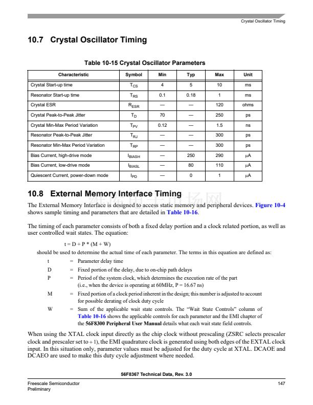
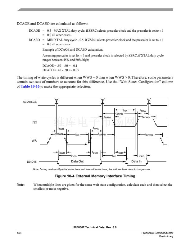
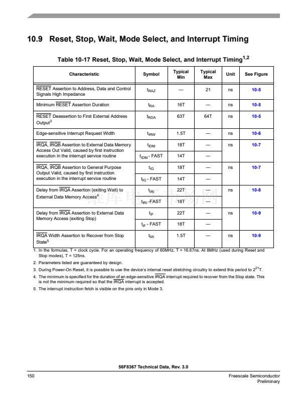
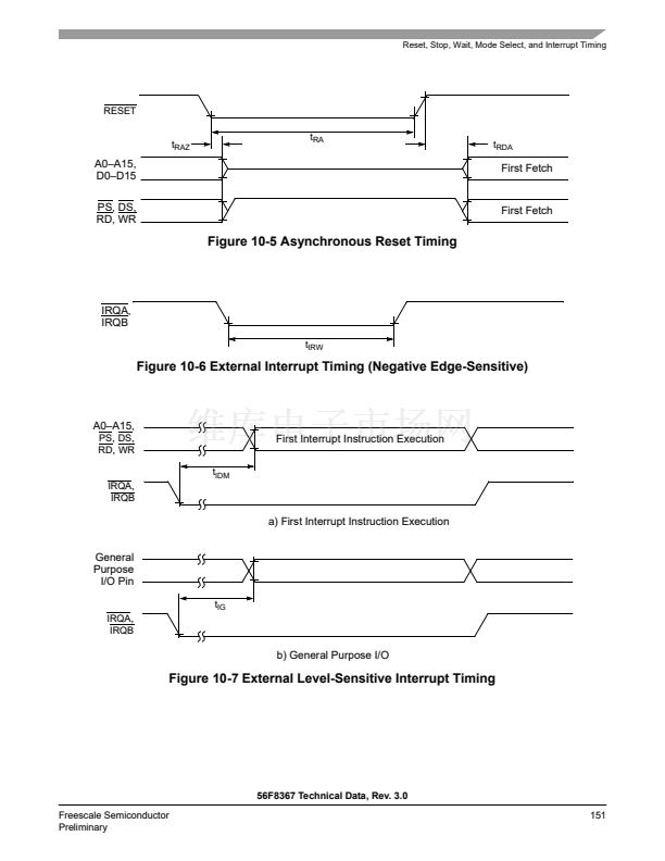
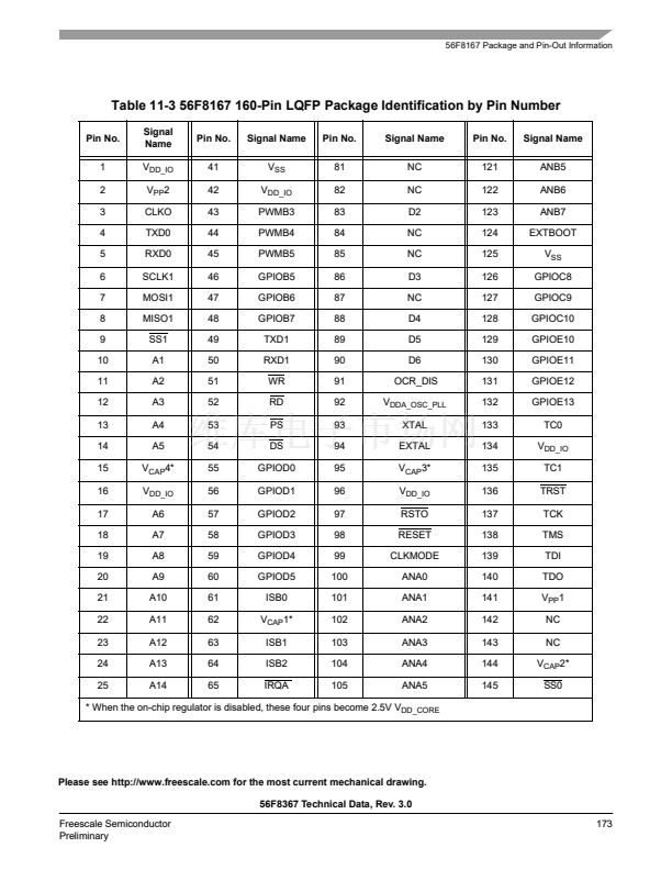
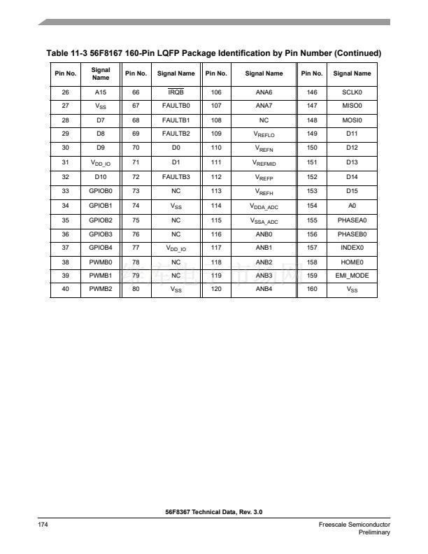
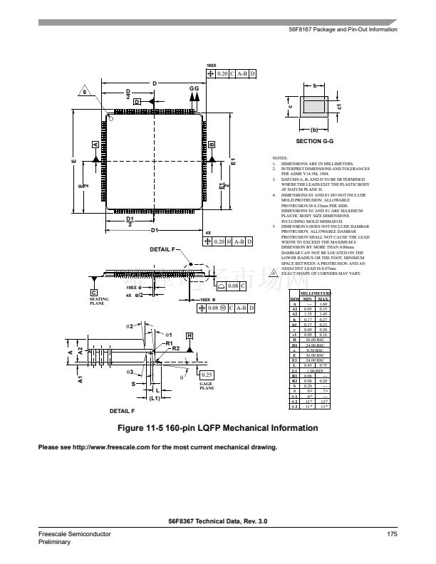
Table 2-2 Signal and Package Information for the 160-Pin LQFP and MBGA
Signal
Name
CLKO
Pin
No.
3
Ball No.
Type
State
During
Reset
Signal Description
D3
Output
Tri-Stated
Clock Output
鈥?This pin outputs a buffered clock signal. Using the
SIM CLKO Select Register (SIM_CLKOSR), this pin can be
programmed as any of the following: disabled, CLK_MSTR (system
clock), IPBus clock, oscillator output, prescaler clock and postscaler
clock. Other signals are also available for test purposes.
See
Part 6.5.7
for details.
A0
154
C3
Output
Tri-stated
Address Bus
鈥?A0 - A5 specify six of the address lines for external
program or data memory accesses.
Depending upon the state of the DRV bit in the EMI bus control register
(BCR), A0 - A5 and EMI control signals are tri-stated when the external
bus is inactive.
Most designs will want to change the DRV state to DRV = 1 instead of
using the default setting.
(GPIOA8)
A1
(GPIOA9)
A2
(GPIOA10)
A3
(GPIOA11)
A4
(GPIOA12)
A5
(GPIOA13)
A6
10
E3
Input/
Output
Input
Port A GPIO
鈥?These six GPIO pins can be individually programmed
as input or output pins.
After reset, the default state is Address Bus.
11
E4
To deactivate the internal pull-up resistor, clear the appropriate GPIO
bit in the GPIOA_PUR register.
Example: GPIOA8, clear bit 8 in the GPIOA_PUR register.
12
F2
13
F1
14
F3
17
G1
Output
Tri-stated
Address Bus
鈥?A6 - A7 specify two of the address lines for external
program or data memory accesses.
Depending upon the state of the DRV bit in the EMI bus control register
(BCR), A6 - A7 and EMI control signals are tri-stated when the external
bus is inactive.
Most designs will want to change the DRV state to DRV = 1 instead of
using the default setting.
(GPIOE2)
A7
(GPIOE3)
18
G3
Schmitt
Input/
Output
Input
Port E GPIO
鈥?These two GPIO pins can be individually programmed
as input or output pins.
After reset, the default state is Address Bus.
To deactivate the internal pull-up resistor, clear the appropriate GPIO
bit in the GPIOE_PUR register.
Example: GPIOE2, clear bit 2 in the GPIOE_PUR register.
56F8367 Technical Data, Rev. 3.0
20
Freescale Semiconductor
Preliminary


 1
1
 2
2
 3
3
 4
4
 5
5
 6
6
 7
7
 8
8
 9
9
 10
10
 11
11
 12
12
 13
13
 14
14
 15
15
 16
16
 17
17
 18
18
 19
19
 20
20
 21
21
 22
22
 23
23
 24
24
 25
25
 26
26
 27
27
 28
28
 29
29
 30
30
 31
31
 32
32
 33
33
 34
34
 35
35
 36
36
 37
37
 38
38
 39
39
 40
40
 41
41
 42
42
 43
43
 44
44
 45
45
 46
46
 47
47
 48
48
 49
49
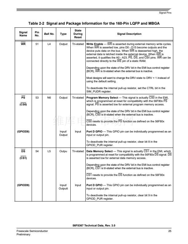
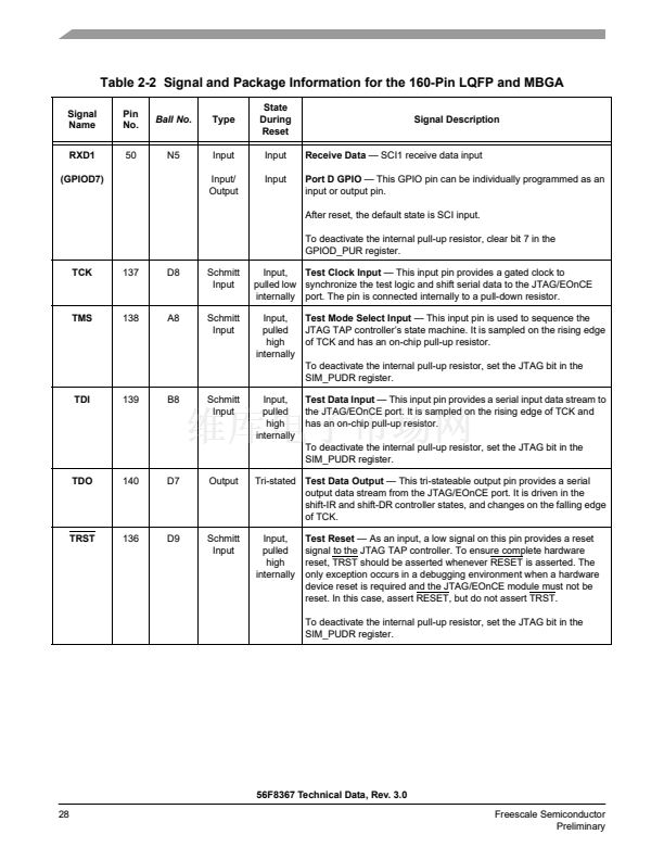
 50
50
 51
51
 52
52
 53
53
 54
54
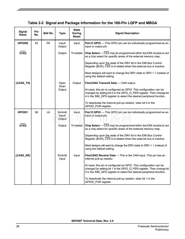
 55
55
 56
56
 57
57
 58
58
 59
59
 60
60
 61
61
 62
62
 63
63
 64
64
 65
65
 66
66
 67
67
 68
68
 69
69
 70
70
 71
71
 72
72
 73
73
 74
74
 75
75
 76
76
 77
77
 78
78
 79
79
 80
80
 81
81
 82
82
 83
83
 84
84
 85
85
 86
86
 87
87
 88
88
 89
89
 90
90
 91
91
 92
92
 93
93
 94
94
 95
95
 96
96
 97
97
 98
98
 99
99
 100
100
 101
101
 102
102
 103
103
 104
104
 105
105
 106
106
 107
107
 108
108
 109
109
 110
110
 111
111
 112
112
 113
113
 114
114
 115
115
 116
116
 117
117
 118
118
 119
119
 120
120
 121
121
 122
122
 123
123
 124
124
 125
125
 126
126
 127
127
 128
128
 129
129
 130
130
 131
131
 132
132
 133
133
 134
134
 135
135
 136
136
 137
137
 138
138
 139
139
 140
140
 141
141
 142
142
 143
143
 144
144
 145
145
 146
146
 147
147
 148
148
 149
149
 150
150
 151
151
 152
152
 153
153
 154
154
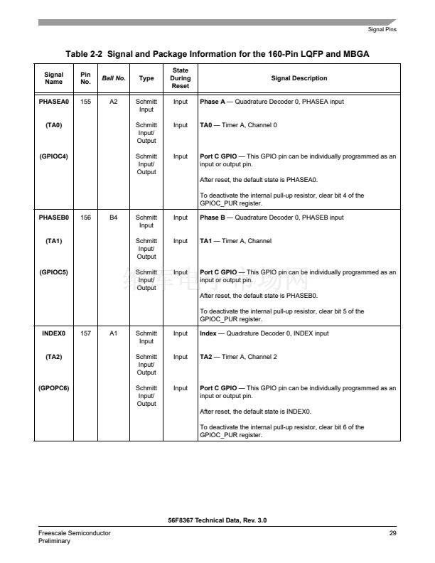
 155
155
 156
156
 157
157
 158
158
 159
159
 160
160
 161
161
 162
162
 163
163
 164
164
 165
165
 166
166
 167
167
 168
168
 169
169
 170
170
 171
171
 172
172
 173
173
 174
174
 175
175
 176
176
 177
177
 178
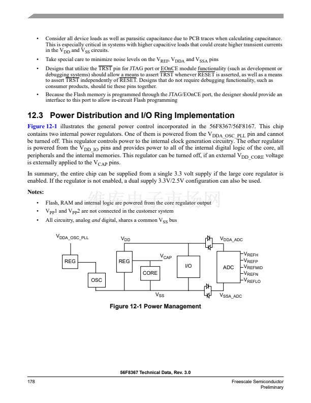
178
 179
179
 180
180
