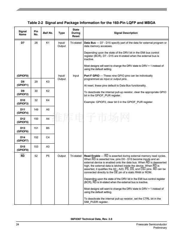
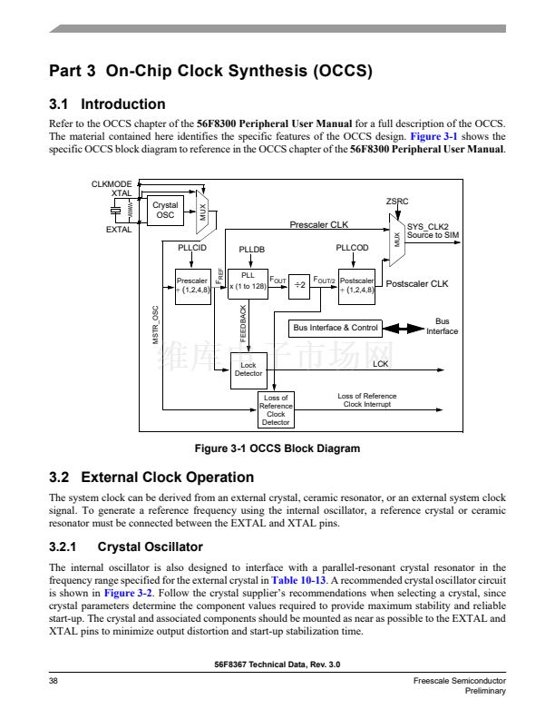
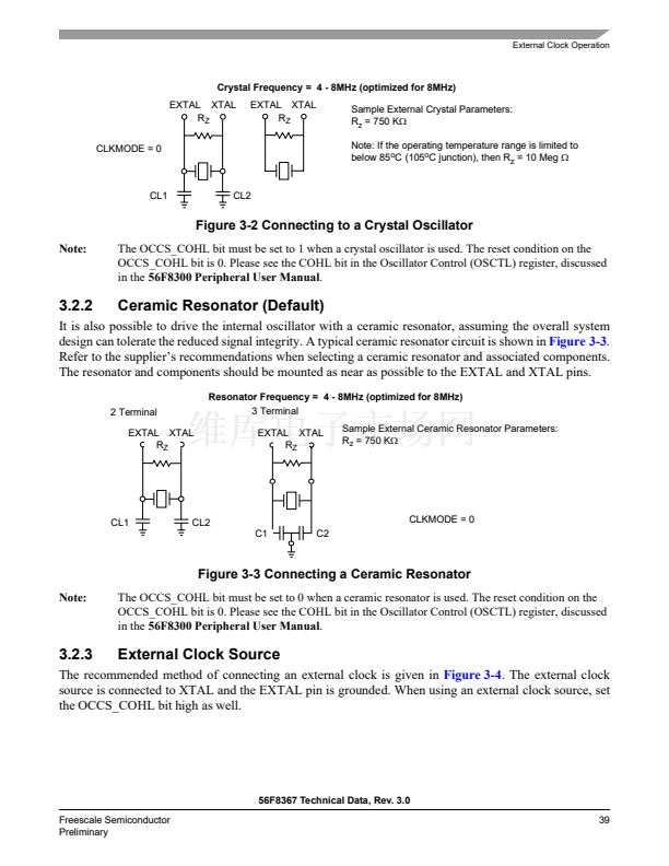
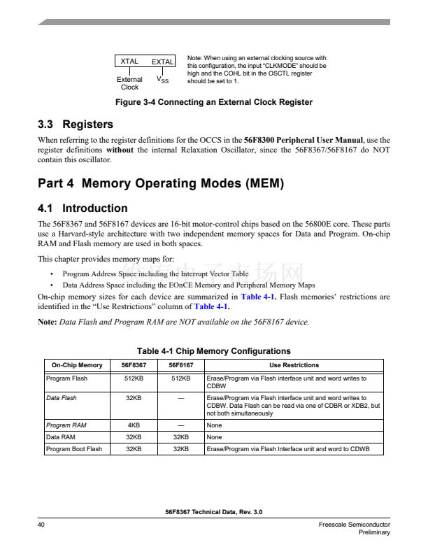
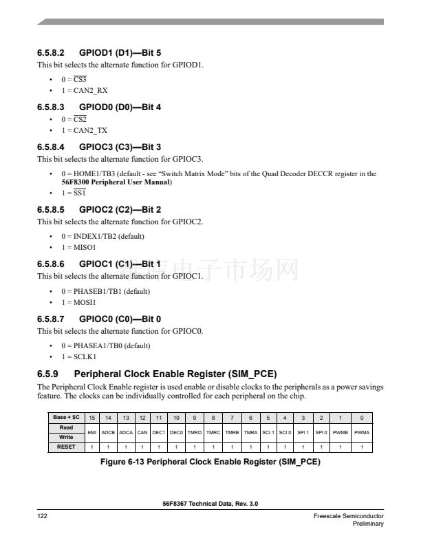
XTAL
External
Clock
EXTAL
V
SS
Note: When using an external clocking source with
this configuration, the input 鈥淐LKMODE鈥?should be
high and the COHL bit in the OSCTL register
should be set to 1.
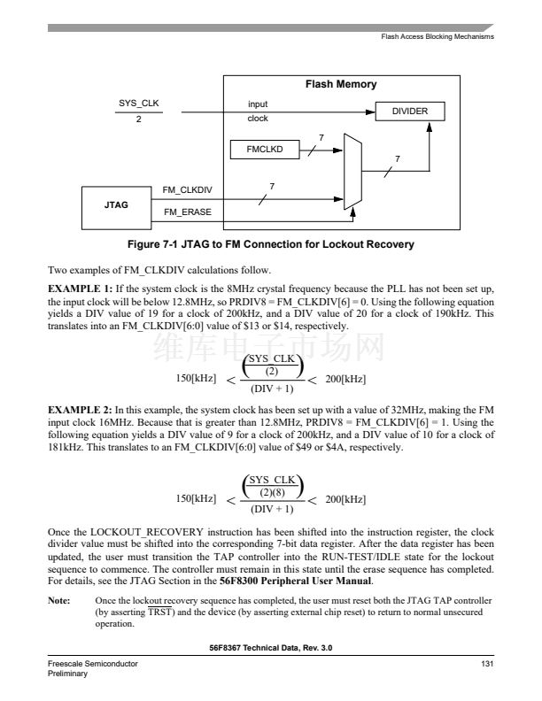
Figure 3-4 Connecting an External Clock Register
3.3 Registers
When referring to the register definitions for the OCCS in the
56F8300 Peripheral User Manual,
use the
register definitions
without
the internal Relaxation Oscillator, since the 56F8367/56F8167 do NOT
contain this oscillator.
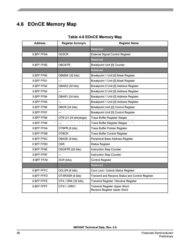
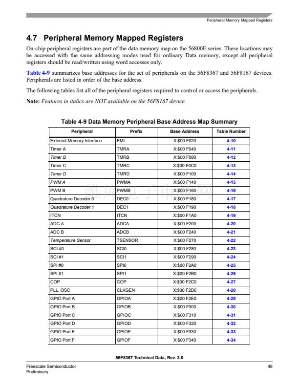
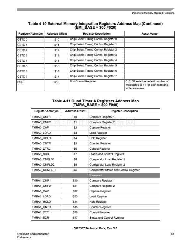
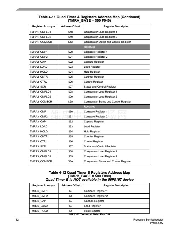
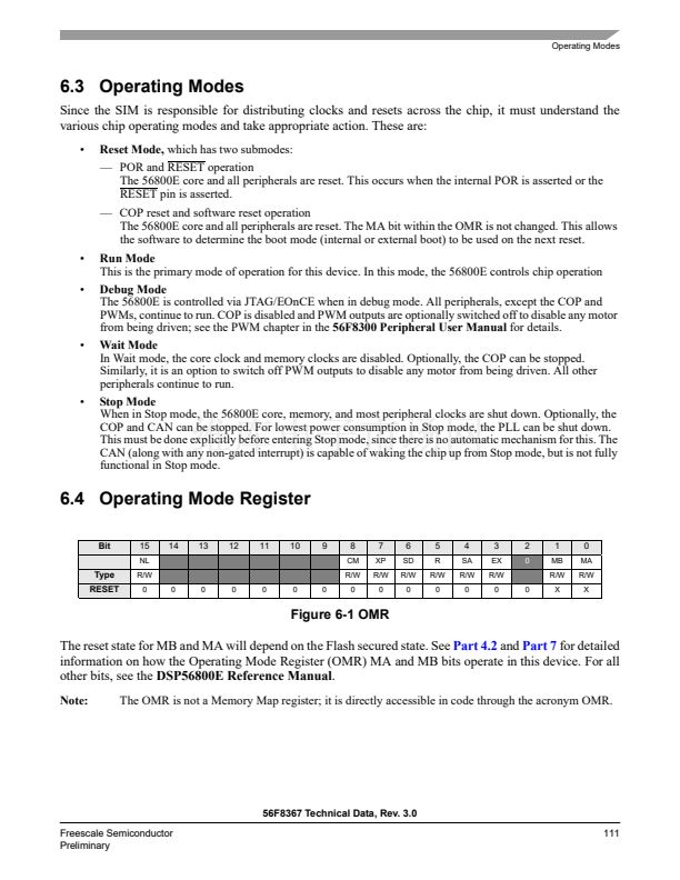
Part 4 Memory Operating Modes (MEM)
4.1 Introduction
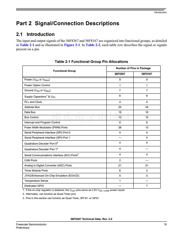
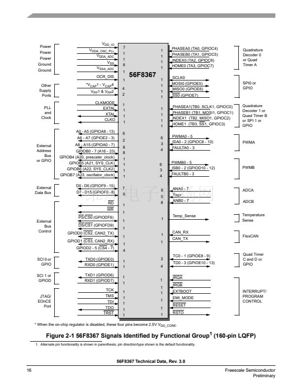
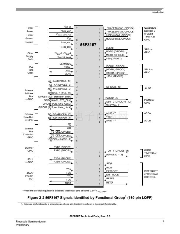
The 56F8367 and 56F8167 devices are 16-bit motor-control chips based on the 56800E core. These parts
use a Harvard-style architecture with two independent memory spaces for Data and Program. On-chip
RAM and Flash memory are used in both spaces.
This chapter provides memory maps for:
鈥?/div>
鈥?/div>
Program Address Space including the Interrupt Vector Table
Data Address Space including the EOnCE Memory and Peripheral Memory Maps
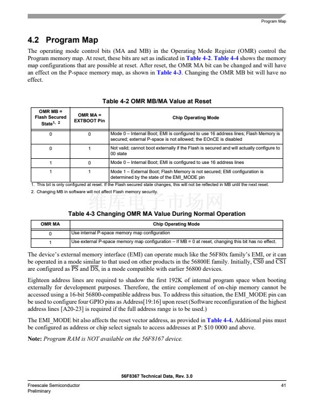
On-chip memory sizes for each device are summarized in
Table 4-1.
Flash memories鈥?restrictions are
identified in the 鈥淯se Restrictions鈥?column of
Table 4-1.
Note:
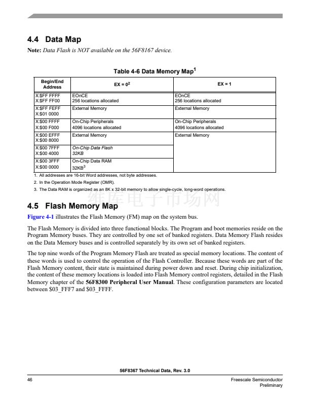
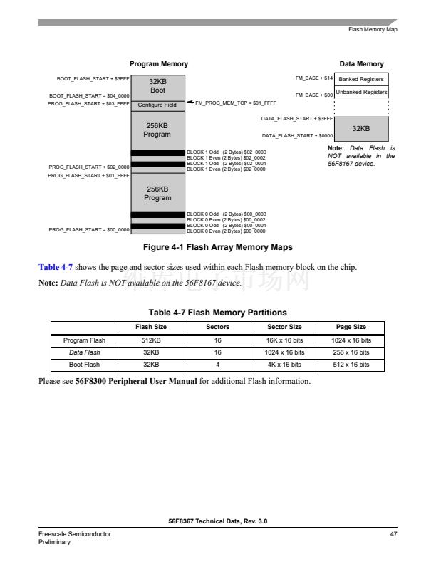
Data Flash and Program RAM are NOT available on the 56F8167 device.
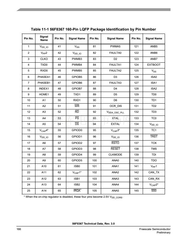
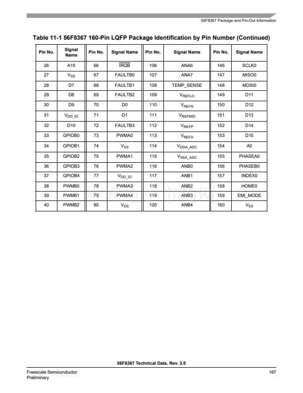
Table 4-1 Chip Memory Configurations
On-Chip Memory
Program Flash
Data Flash
56F8367
512KB
32KB
56F8167
512KB
鈥?/div>
Use Restrictions
Erase/Program via Flash interface unit and word writes to
CDBW
Erase/Program via Flash interface unit and word writes to
CDBW. Data Flash can be read via one of CDBR or XDB2, but
not both simultaneously
None
None
Erase/Program via Flash Interface unit and word to CDWB
Program RAM
Data RAM
Program Boot Flash
4KB
32KB
32KB
鈥?/div>
32KB
32KB
56F8367 Technical Data, Rev. 3.0
40
Freescale Semiconductor
Preliminary


 1
1
 2
2
 3
3
 4
4
 5
5
 6
6
 7
7
 8
8
 9
9
 10
10
 11
11
 12
12
 13
13
 14
14
 15
15
 16
16
 17
17
 18
18
 19
19
 20
20
 21
21
 22
22
 23
23
 24
24
 25
25
 26
26
 27
27
 28
28
 29
29
 30
30
 31
31
 32
32
 33
33
 34
34
 35
35
 36
36
 37
37
 38
38
 39
39
 40
40
 41
41
 42
42
 43
43
 44
44
 45
45
 46
46
 47
47
 48
48
 49
49
 50
50
 51
51
 52
52
 53
53
 54
54
 55
55
 56
56
 57
57
 58
58
 59
59
 60
60
 61
61
 62
62
 63
63
 64
64
 65
65
 66
66
 67
67
 68
68
 69
69
 70
70
 71
71
 72
72
 73
73
 74
74
 75
75
 76
76
 77
77
 78
78
 79
79
 80
80
 81
81
 82
82
 83
83
 84
84
 85
85
 86
86
 87
87
 88
88
 89
89
 90
90
 91
91
 92
92
 93
93
 94
94
 95
95
 96
96
 97
97
 98
98
 99
99
 100
100
 101
101
 102
102
 103
103
 104
104
 105
105
 106
106
 107
107
 108
108
 109
109
 110
110
 111
111
 112
112
 113
113
 114
114
 115
115
 116
116
 117
117
 118
118
 119
119
 120
120
 121
121
 122
122
 123
123
 124
124
 125
125
 126
126
 127
127
 128
128
 129
129
 130
130
 131
131
 132
132
 133
133
 134
134
 135
135
 136
136
 137
137
 138
138
 139
139
 140
140
 141
141
 142
142
 143
143
 144
144
 145
145
 146
146
 147
147
 148
148
 149
149
 150
150
 151
151
 152
152
 153
153
 154
154
 155
155
 156
156
 157
157
 158
158
 159
159
 160
160
 161
161
 162
162
 163
163
 164
164
 165
165
 166
166
 167
167
 168
168
 169
169
 170
170
 171
171
 172
172
 173
173
 174
174
 175
175
 176
176
 177
177
 178
178
 179
179
 180
180
