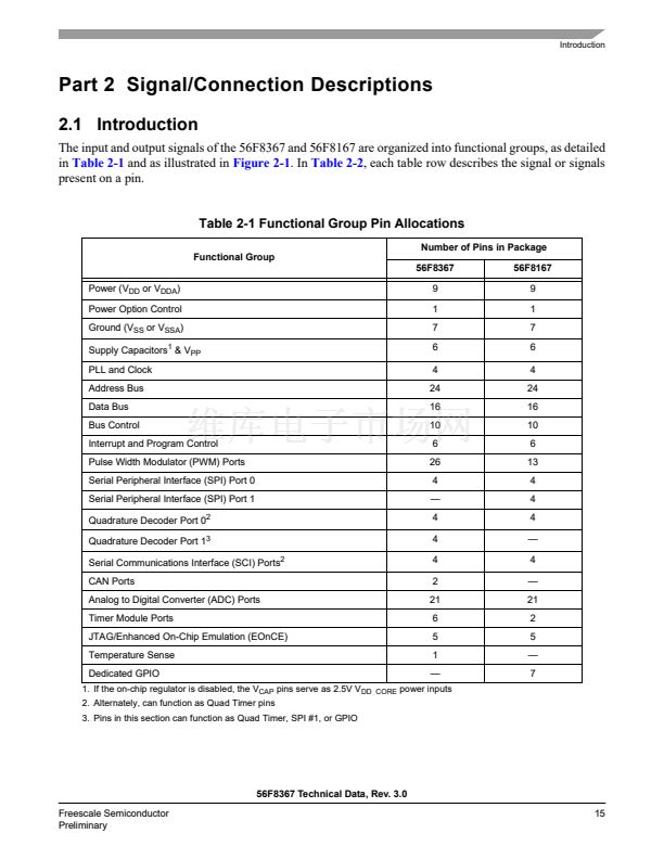
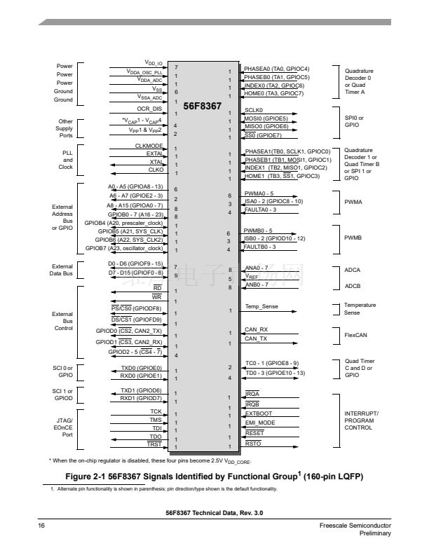
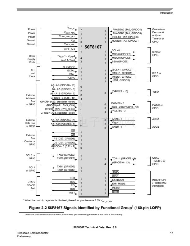
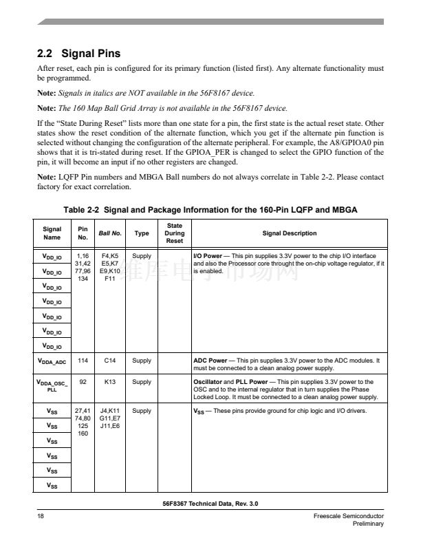
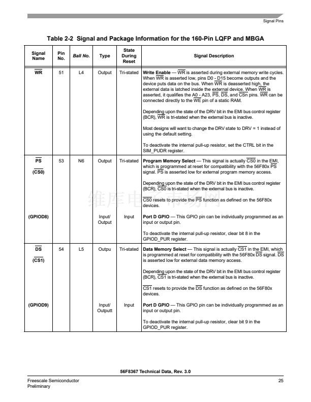
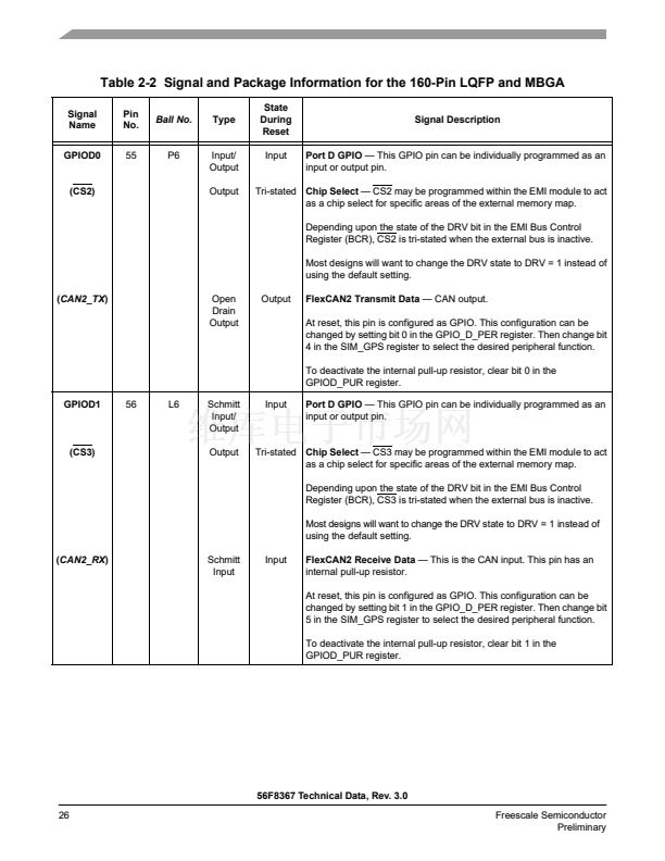
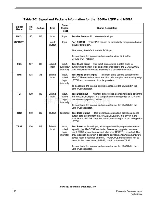
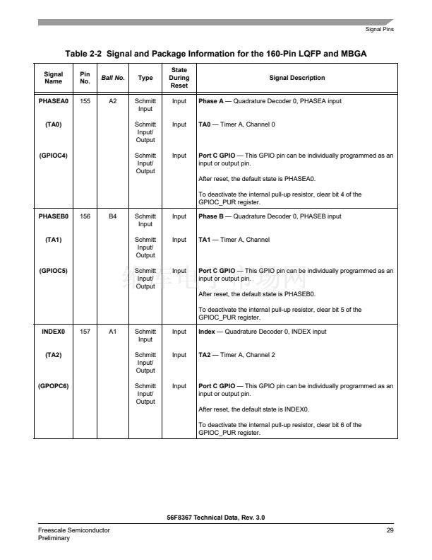
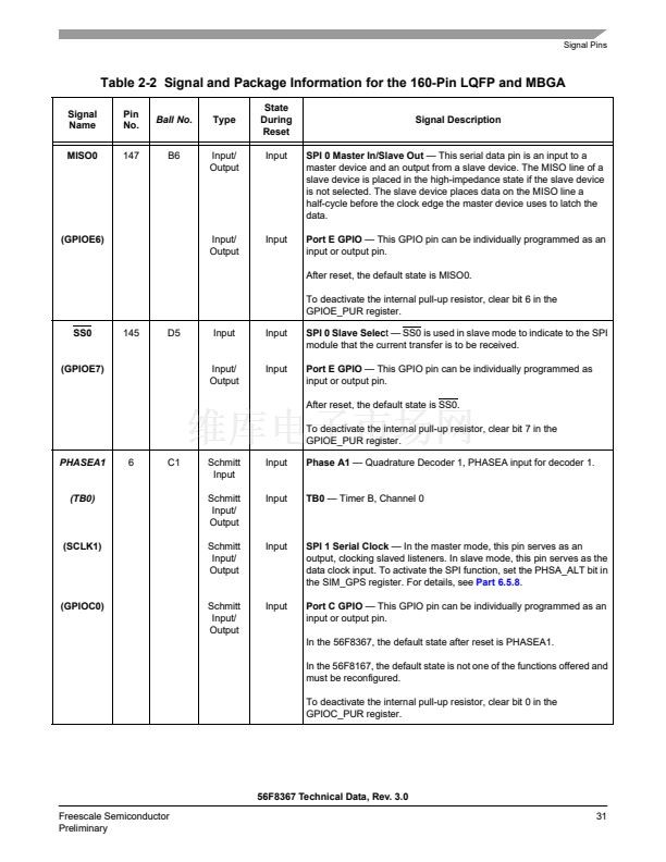
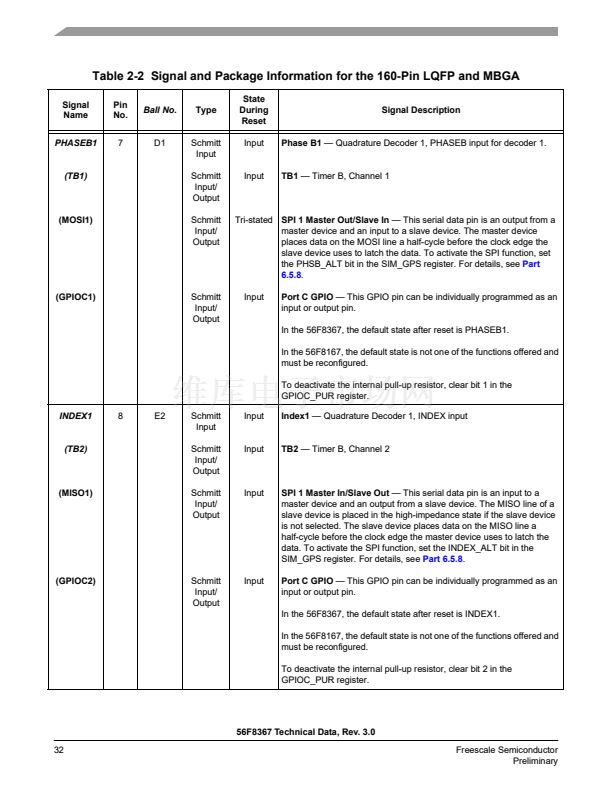
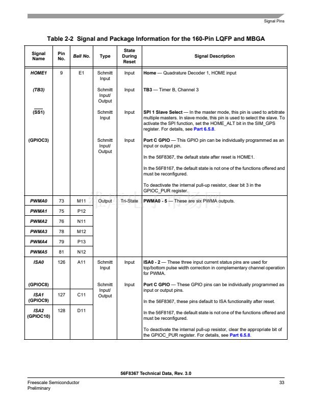
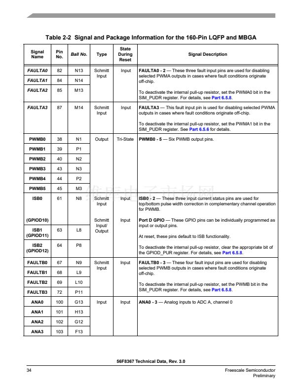
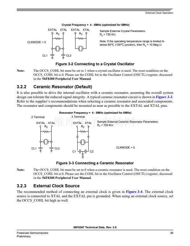
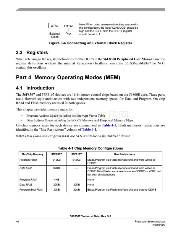
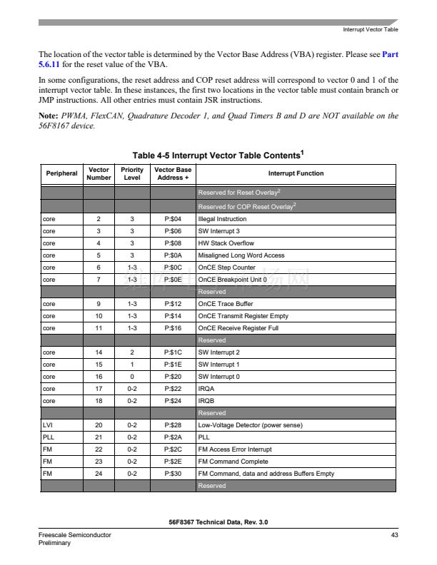
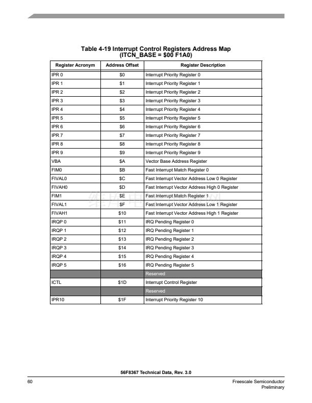
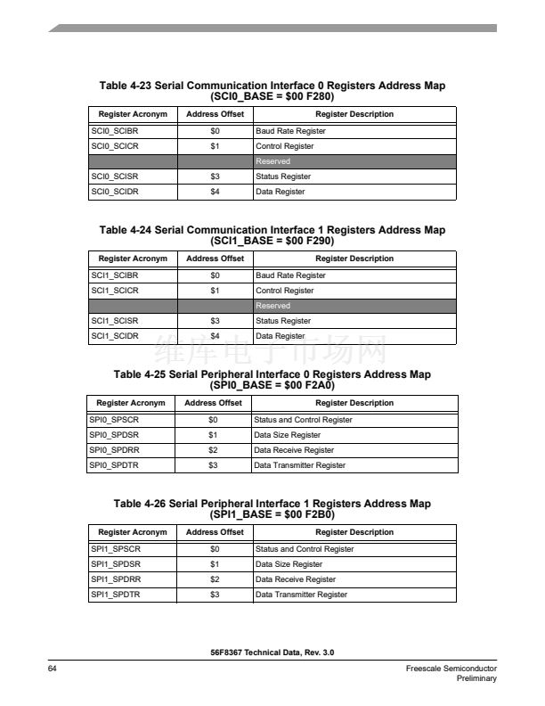
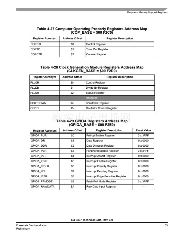
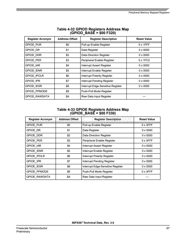
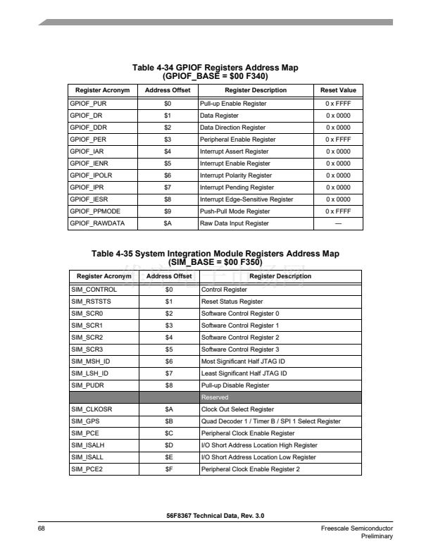
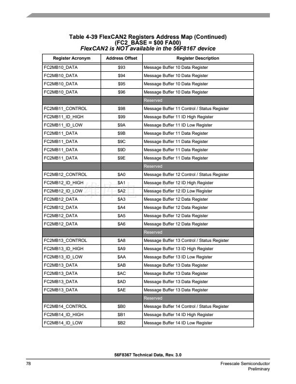
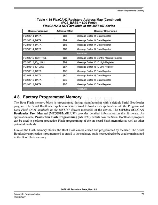
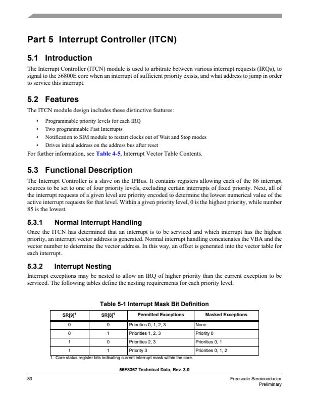
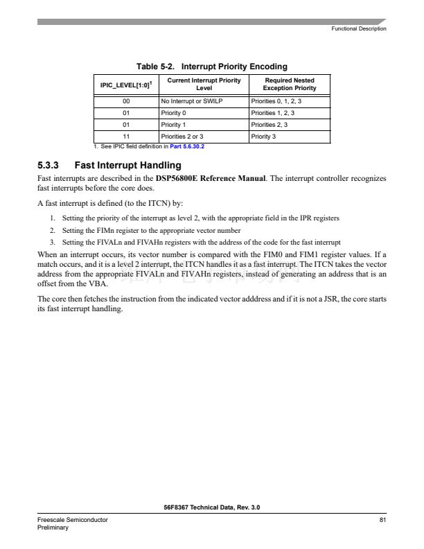
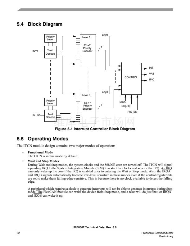
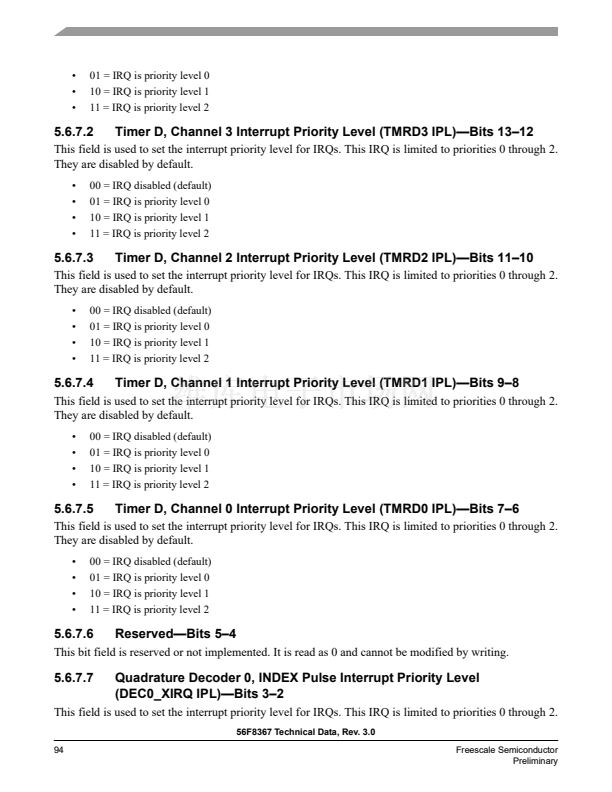
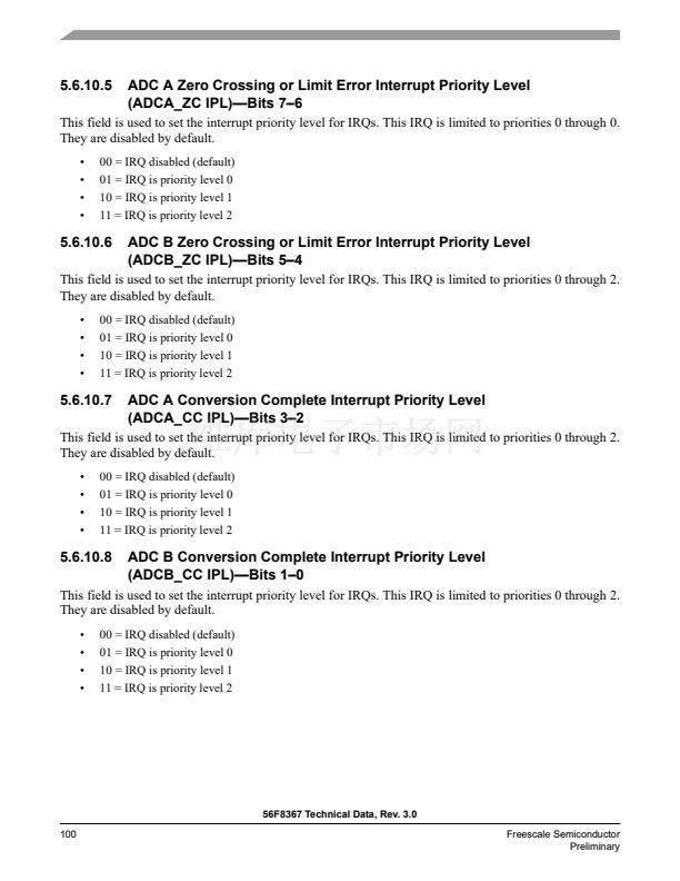
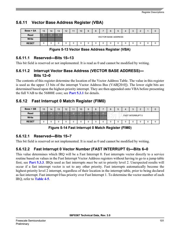
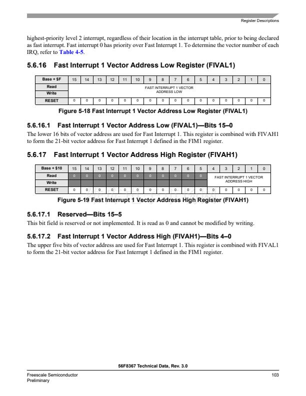
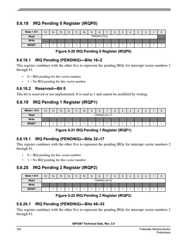
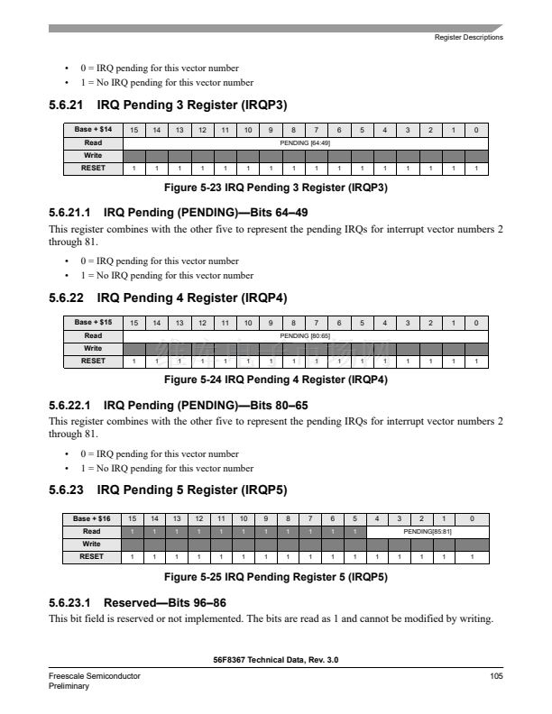
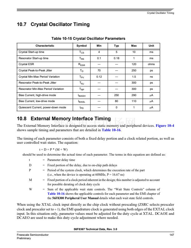
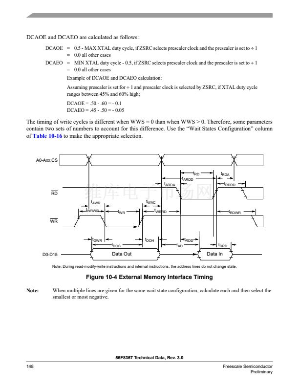
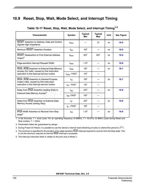
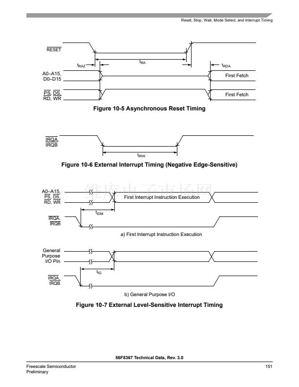
Interrupt Vector Table
The location of the vector table is determined by the Vector Base Address (VBA) register. Please see
Part
5.6.11
for the reset value of the VBA.
In some configurations, the reset address and COP reset address will correspond to vector 0 and 1 of the
interrupt vector table. In these instances, the first two locations in the vector table must contain branch or
JMP instructions. All other entries must contain JSR instructions.
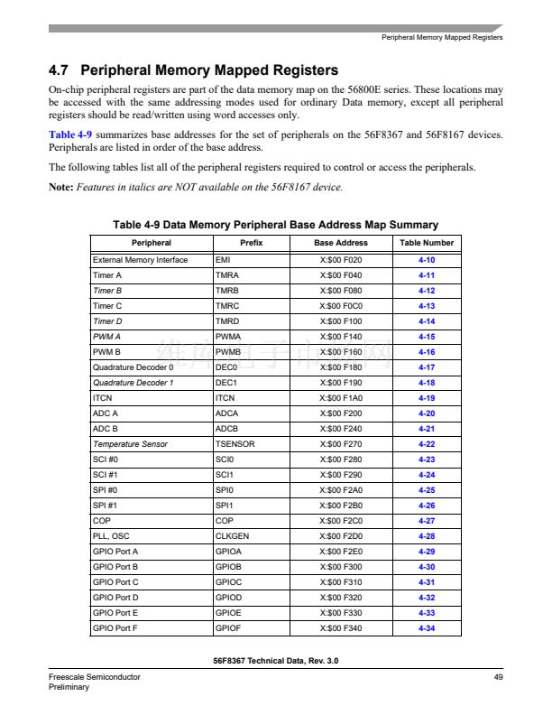
Note:
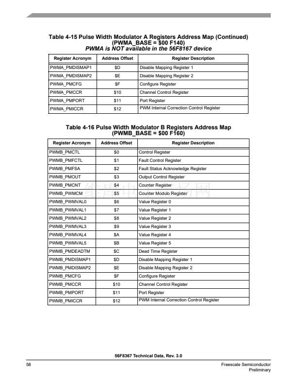
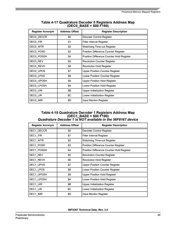
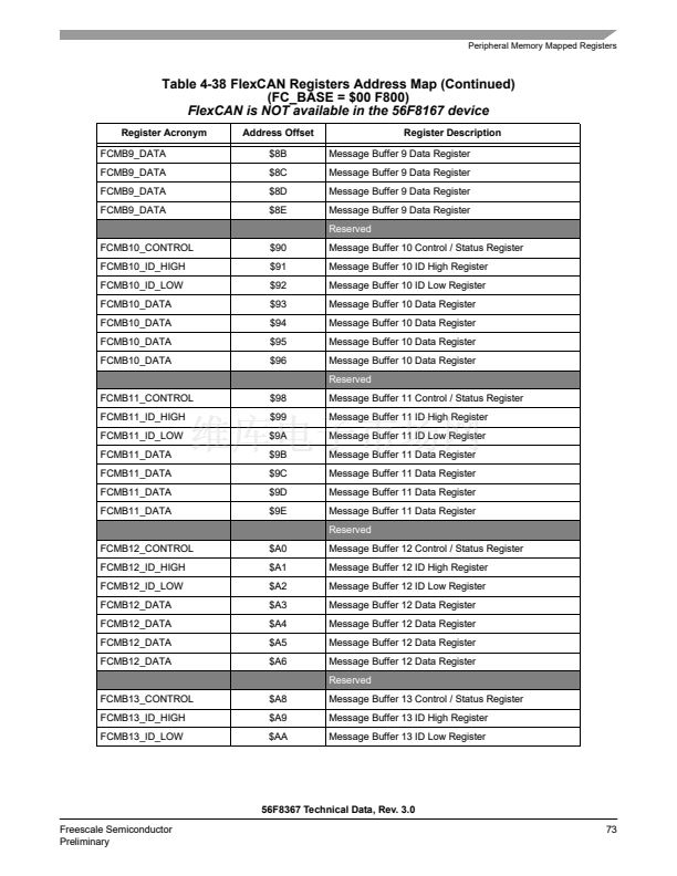
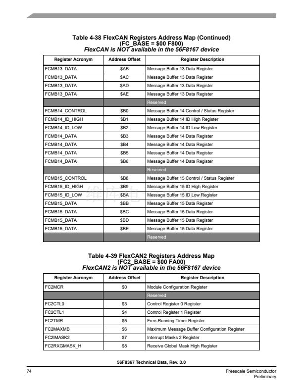
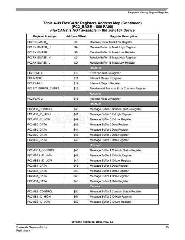
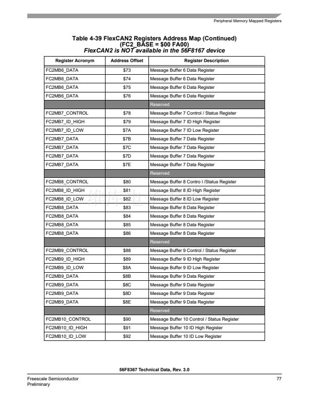
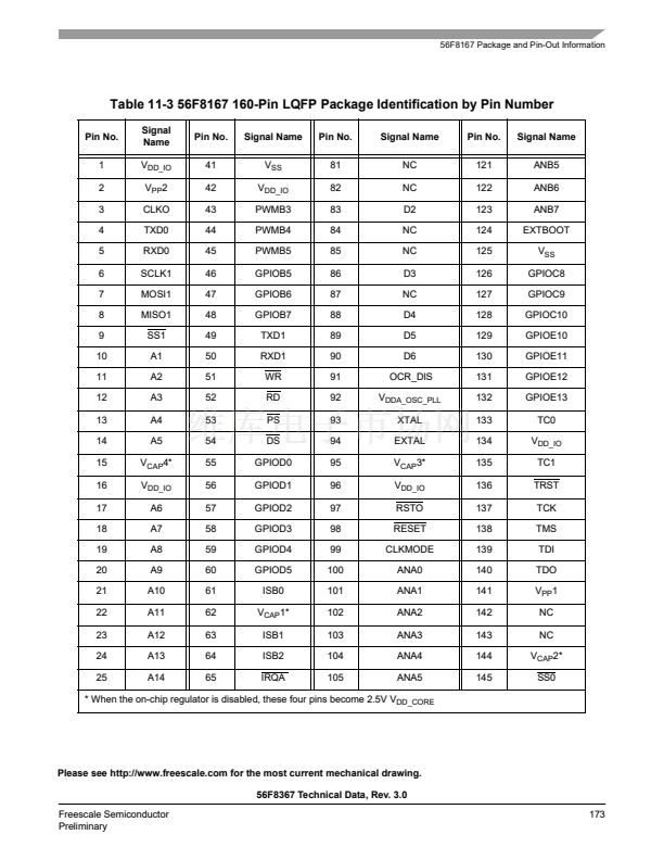
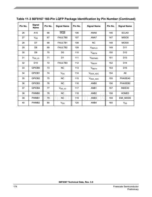
PWMA, FlexCAN, Quadrature Decoder 1, and Quad Timers B and D are NOT available on the
56F8167 device.
Table 4-5 Interrupt Vector Table Contents
1
Peripheral
Vector
Number
Priority
Level
Vector Base
Address +
Interrupt Function
Reserved for Reset Overlay
2
Reserved for COP Reset Overlay
2
core
core
core
core
core
core
2
3
4
5
6
7
3
3
3
3
1-3
1-3
P:$04
P:$06
P:$08
P:$0A
P:$0C
P:$0E
Illegal Instruction
SW Interrupt 3
HW Stack Overflow
Misaligned Long Word Access
OnCE Step Counter
OnCE Breakpoint Unit 0
Reserved
core
core
core
9
10
11
1-3
1-3
1-3
P:$12
P:$14
P:$16
OnCE Trace Buffer
OnCE Transmit Register Empty
OnCE Receive Register Full
Reserved
core
core
core
core
core
14
15
16
17
18
2
1
0
0-2
0-2
P:$1C
P:$1E
P:$20
P:$22
P:$24
SW Interrupt 2
SW Interrupt 1
SW Interrupt 0
IRQA
IRQB
Reserved
LVI
PLL
FM
FM
FM
20
21
22
23
24
0-2
0-2
0-2
0-2
0-2
P:$28
P:$2A
P:$2C
P:$2E
P:$30
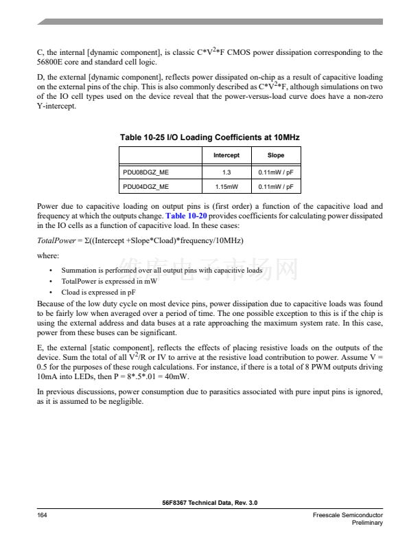
Low-Voltage Detector (power sense)
PLL
FM Access Error Interrupt
FM Command Complete
FM Command, data and address Buffers Empty
Reserved
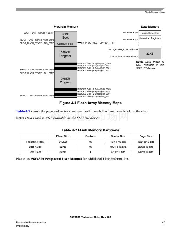
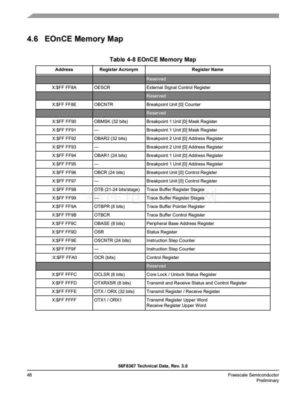
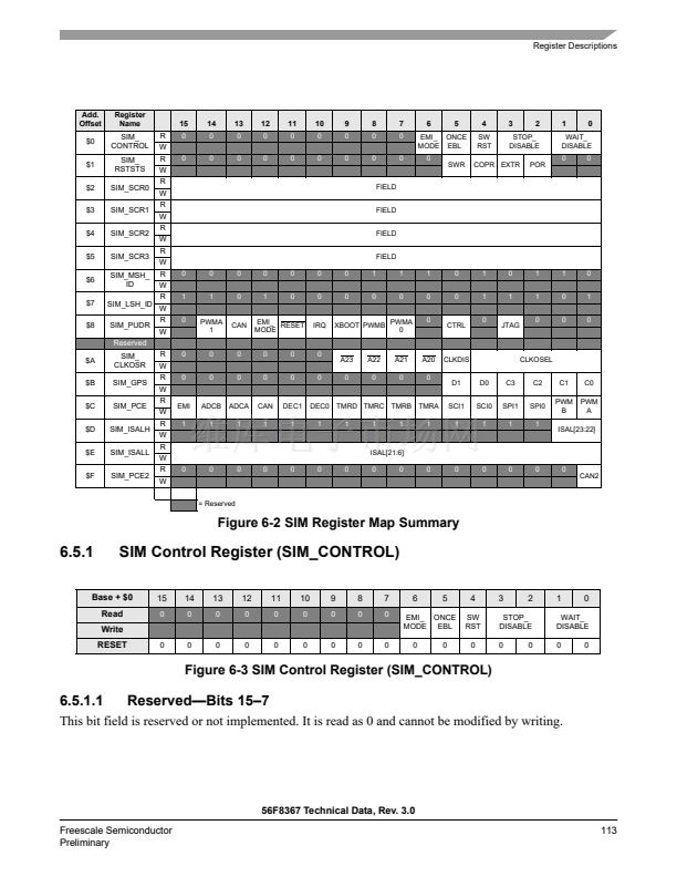
56F8367 Technical Data, Rev. 3.0
Freescale Semiconductor
Preliminary
43


 1
1
 2
2
 3
3
 4
4
 5
5
 6
6
 7
7
 8
8
 9
9
 10
10
 11
11
 12
12
 13
13
 14
14
 15
15
 16
16
 17
17
 18
18
 19
19
 20
20
 21
21
 22
22
 23
23
 24
24
 25
25
 26
26
 27
27
 28
28
 29
29
 30
30
 31
31
 32
32
 33
33
 34
34
 35
35
 36
36
 37
37
 38
38
 39
39
 40
40
 41
41
 42
42
 43
43
 44
44
 45
45
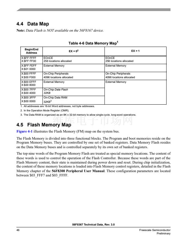 46
46
 47
47
 48
48
 49
49
 50
50
 51
51
 52
52
 53
53
 54
54
 55
55
 56
56
 57
57
 58
58
 59
59
 60
60
 61
61
 62
62
 63
63
 64
64
 65
65
 66
66
 67
67
 68
68
 69
69
 70
70
 71
71
 72
72
 73
73
 74
74
 75
75
 76
76
 77
77
 78
78
 79
79
 80
80
 81
81
 82
82
 83
83
 84
84
 85
85
 86
86
 87
87
 88
88
 89
89
 90
90
 91
91
 92
92
 93
93
 94
94
 95
95
 96
96
 97
97
 98
98
 99
99
 100
100
 101
101
 102
102
 103
103
 104
104
 105
105
 106
106
 107
107
 108
108
 109
109
 110
110
 111
111
 112
112
 113
113
 114
114
 115
115
 116
116
 117
117
 118
118
 119
119
 120
120
 121
121
 122
122
 123
123
 124
124
 125
125
 126
126
 127
127
 128
128
 129
129
 130
130
 131
131
 132
132
 133
133
 134
134
 135
135
 136
136
 137
137
 138
138
 139
139
 140
140
 141
141
 142
142
 143
143
 144
144
 145
145
 146
146
 147
147
 148
148
 149
149
 150
150
 151
151
 152
152
 153
153
 154
154
 155
155
 156
156
 157
157
 158
158
 159
159
 160
160
 161
161
 162
162
 163
163
 164
164
 165
165
 166
166
 167
167
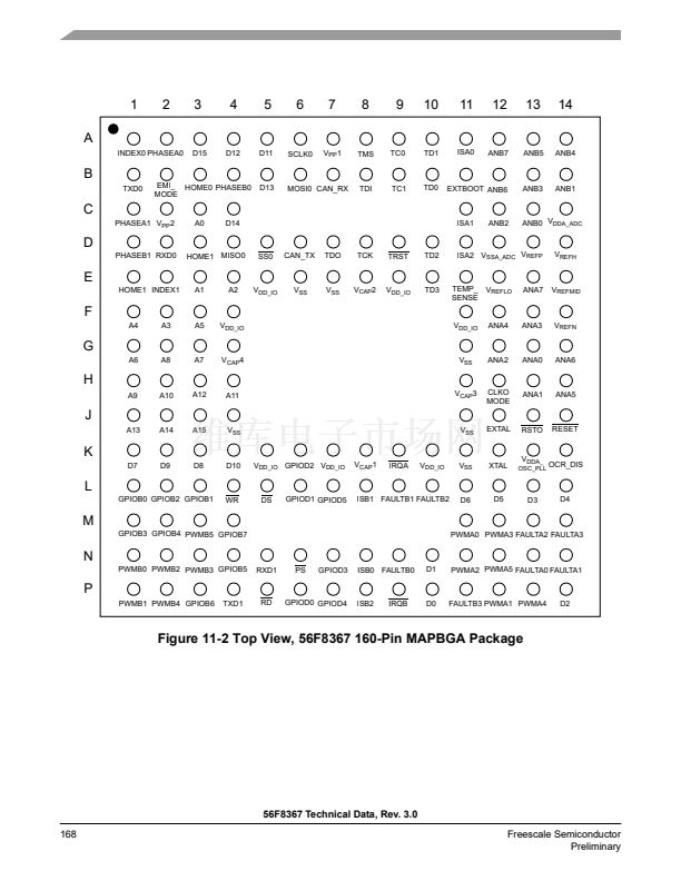 168
168
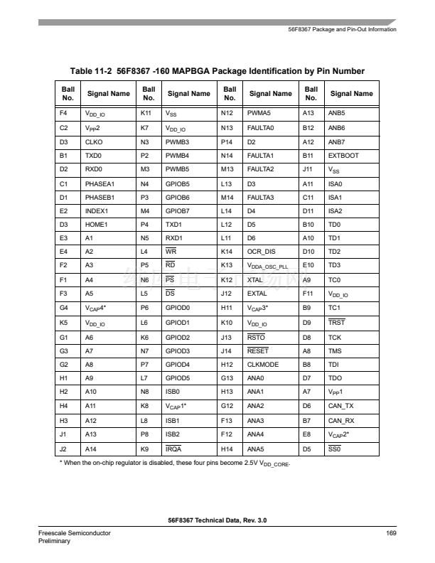 169
169
 170
170
 171
171
 172
172
 173
173
 174
174
 175
175
 176
176
 177
177
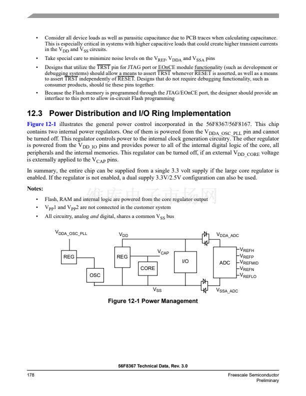 178
178
 179
179
 180
180
