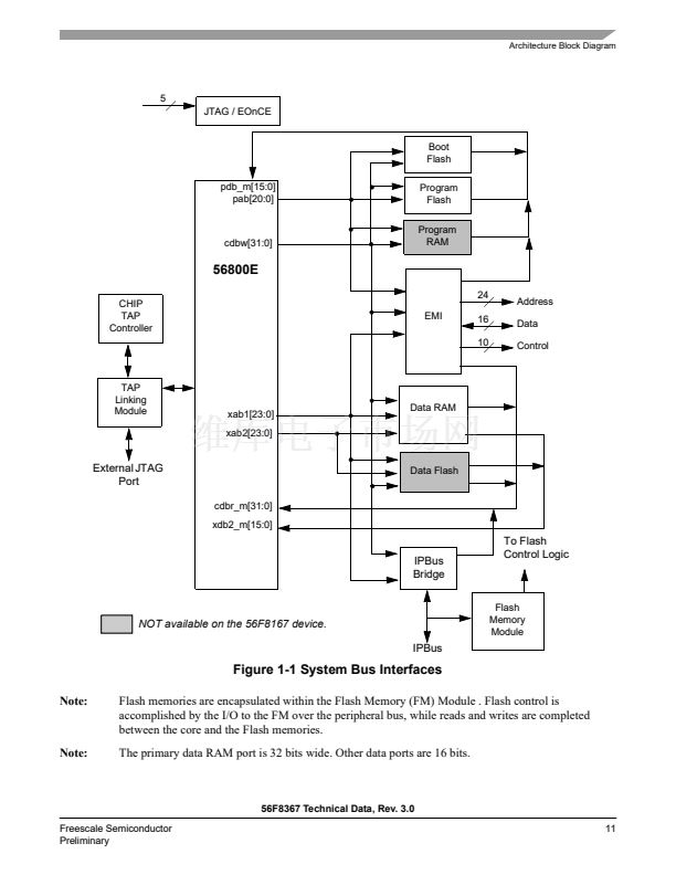
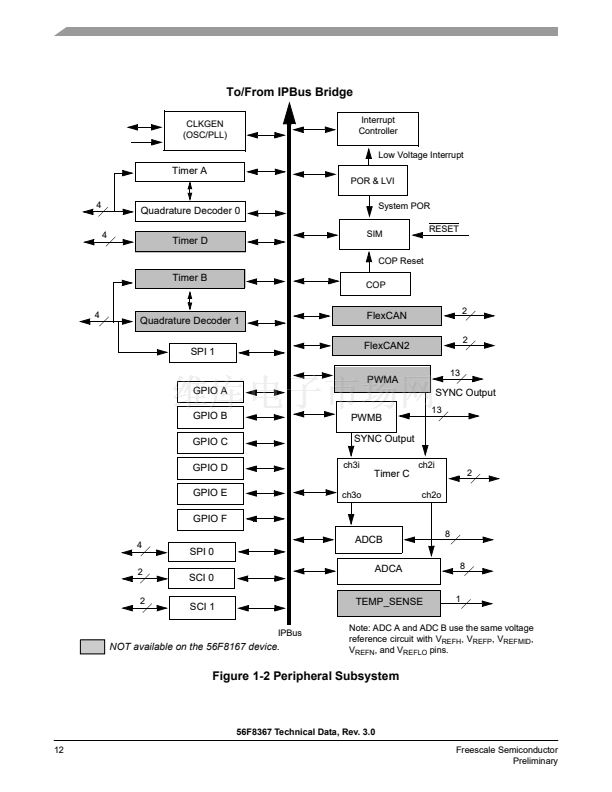
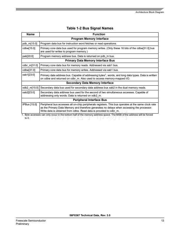
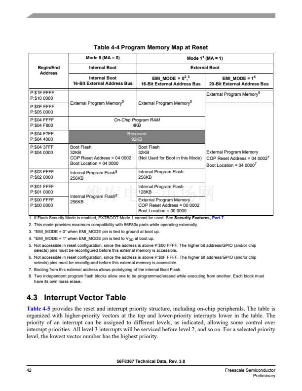
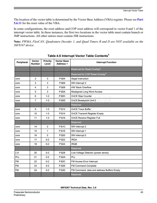
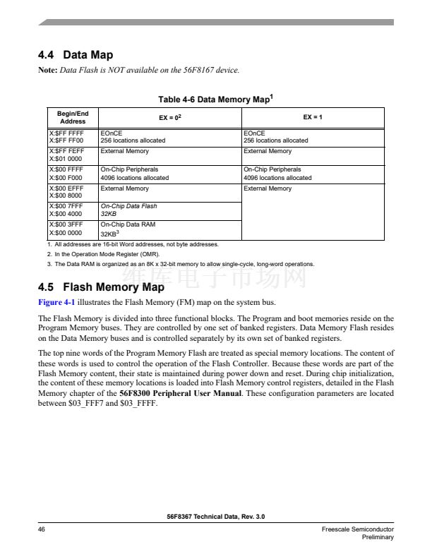
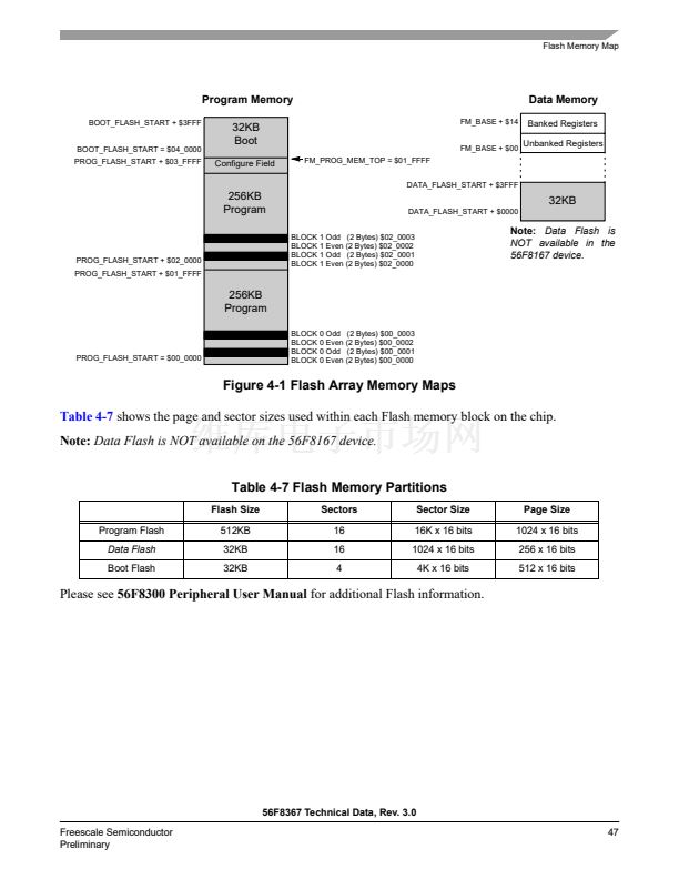
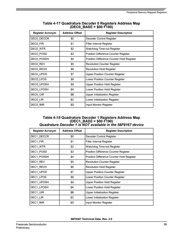
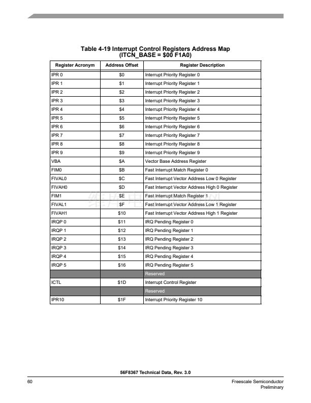
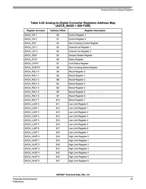
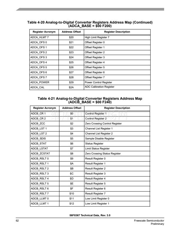
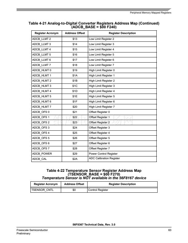
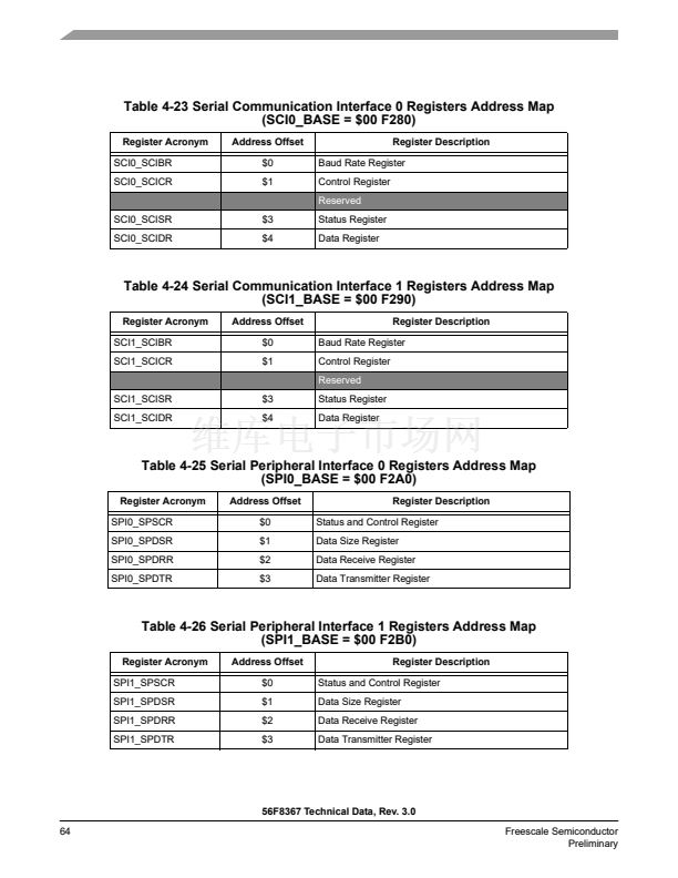
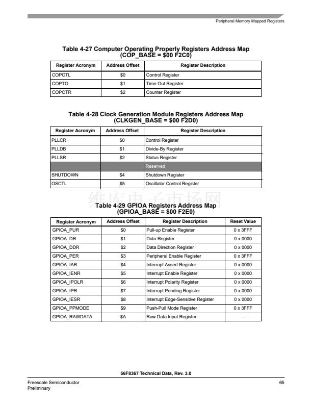
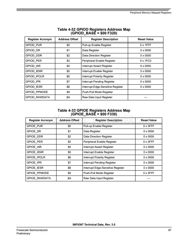
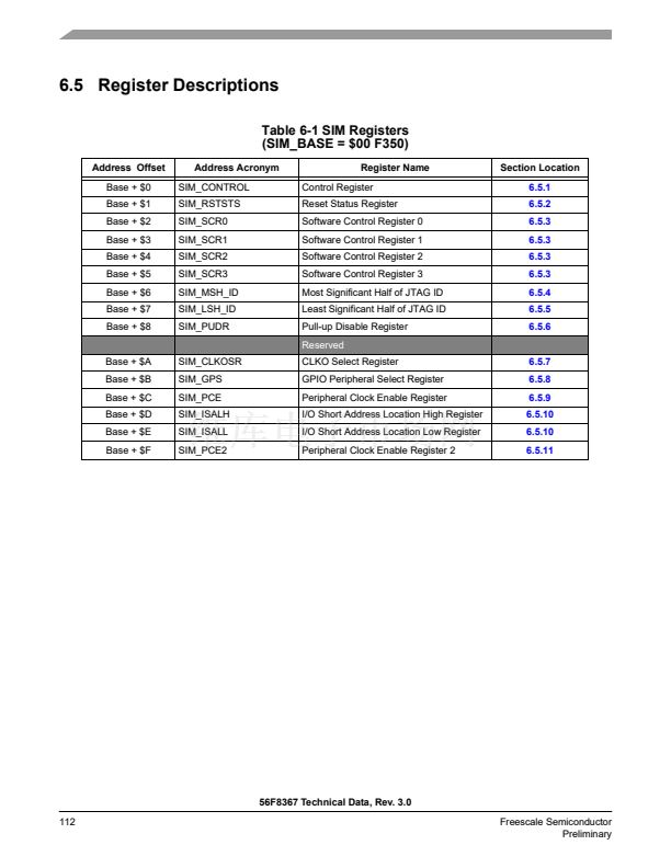
Peripheral Memory Mapped Registers
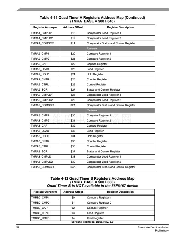
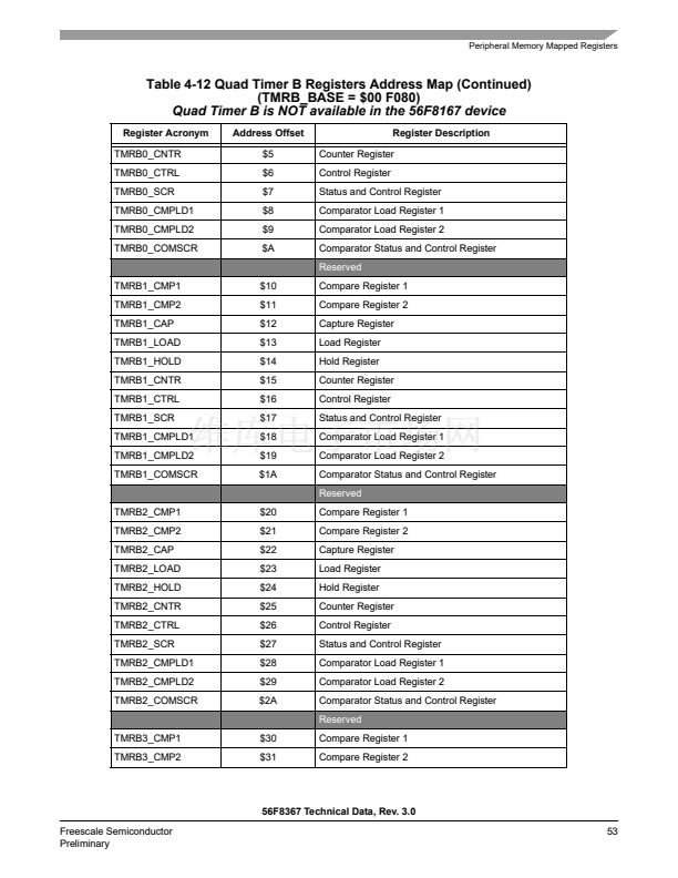
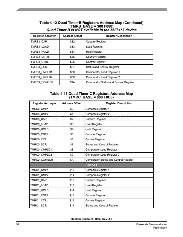
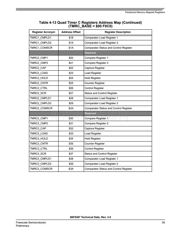
Table 4-14 Quad Timer D Registers Address Map (Continued)
(TMRD_BASE = $00 F100)
Quad Timer D is NOT available in the 56F8167 device
Register Acronym
TMRD2_CMPLD1
TMRD2_CMPLD2
TMRD2_COMSCR
Address Offset
$28
$29
$2A
Register Description
Comparator Load Register 1
Comparator Load Register 2
Comparator Status and Control Register
Reserved
TMRD3_CMP1
TMRD3_CMP2
TMRD3_CAP
TMRD3_LOAD
TMRD3_HOLD
TMRD3_CNTR
TMRD3_CTRL
TMRD3_SCR
TMRD3_CMPLD1
TMRD3_CMPLD2
TMRD3_COMSCR
$30
$31
$32
$33
$34
$35
$36
$37
$38
$39
$3A
Compare Register 1
Compare Register 2
Capture Register
Load Register
Hold Register
Counter Register
Control Register
Status and Control Register
Comparator Load Register 1
Comparator Load Register 2
Comparator Status and Control Register
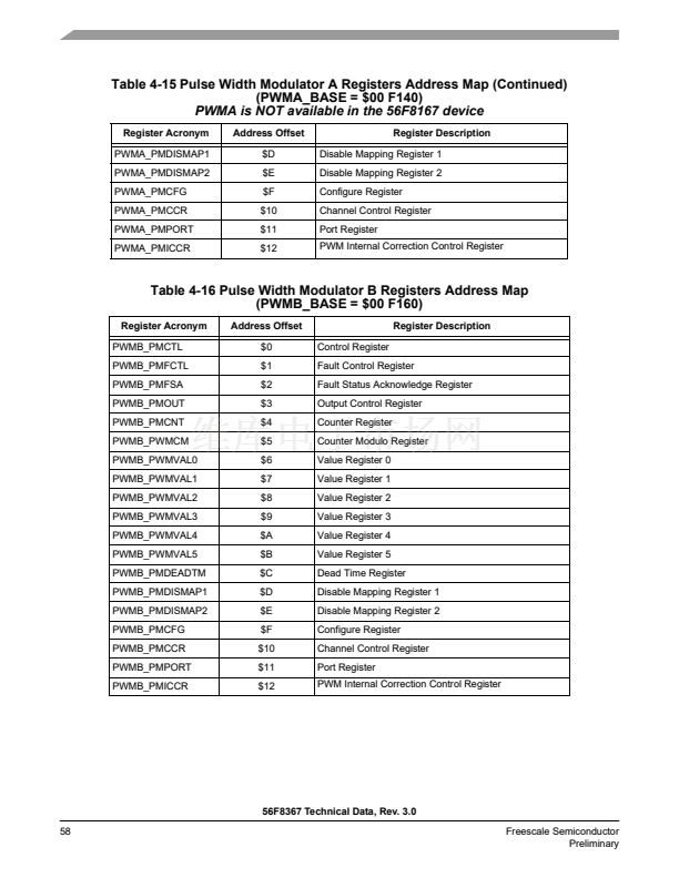
Table 4-15 Pulse Width Modulator A Registers Address Map
(PWMA_BASE = $00 F140)
PWMA is NOT available in the 56F8167 device
Register Acronym
PWMA_PMCTL
PWMA_PMFCTL
PWMA_PMFSA
PWMA_PMOUT
PWMA_PMCNT
PWMA_PWMCM
PWMA_PWMVAL0
PWMA_PWMVAL1
PWMA_PWMVAL2
PWMA_PWMVAL3
PWMA_PWMVAL4
PWMA_PWMVAL5
PWMA_PMDEADTM
Address Offset
$0
$1
$2
$3
$4
$5
$6
$7
$8
$9
$A
$B
$C
Control Register
Fault Control Register
Fault Status Acknowledge Register
Output Control Register
Counter Register
Counter Modulo Register
Value Register 0
Value Register 1
Value Register 2
Value Register 3
Value Register 4
Value Register 5
Dead Time Register
Register Description
56F8367 Technical Data, Rev. 3.0
Freescale Semiconductor
Preliminary
57


 1
1
 2
2
 3
3
 4
4
 5
5
 6
6
 7
7
 8
8
 9
9
 10
10
 11
11
 12
12
 13
13
 14
14
 15
15
 16
16
 17
17
 18
18
 19
19
 20
20
 21
21
 22
22
 23
23
 24
24
 25
25
 26
26
 27
27
 28
28
 29
29
 30
30
 31
31
 32
32
 33
33
 34
34
 35
35
 36
36
 37
37
 38
38
 39
39
 40
40
 41
41
 42
42
 43
43
 44
44
 45
45
 46
46
 47
47
 48
48
 49
49
 50
50
 51
51
 52
52
 53
53
 54
54
 55
55
 56
56
 57
57
 58
58
 59
59
 60
60
 61
61
 62
62
 63
63
 64
64
 65
65
 66
66
 67
67
 68
68
 69
69
 70
70
 71
71
 72
72
 73
73
 74
74
 75
75
 76
76
 77
77
 78
78
 79
79
 80
80
 81
81
 82
82
 83
83
 84
84
 85
85
 86
86
 87
87
 88
88
 89
89
 90
90
 91
91
 92
92
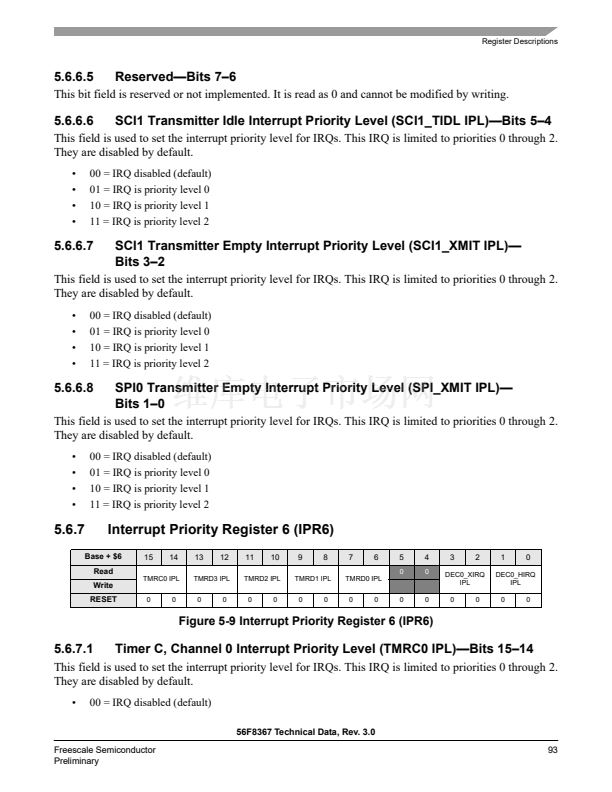 93
93
 94
94
 95
95
 96
96
 97
97
 98
98
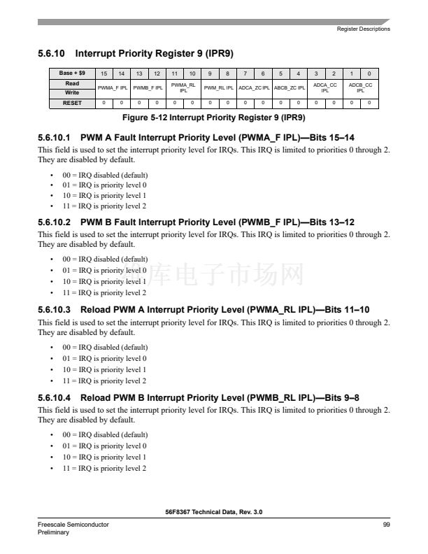 99
99
 100
100
 101
101
 102
102
 103
103
 104
104
 105
105
 106
106
 107
107
 108
108
 109
109
 110
110
 111
111
 112
112
 113
113
 114
114
 115
115
 116
116
 117
117
 118
118
 119
119
 120
120
 121
121
 122
122
 123
123
 124
124
 125
125
 126
126
 127
127
 128
128
 129
129
 130
130
 131
131
 132
132
 133
133
 134
134
 135
135
 136
136
 137
137
 138
138
 139
139
 140
140
 141
141
 142
142
 143
143
 144
144
 145
145
 146
146
 147
147
 148
148
 149
149
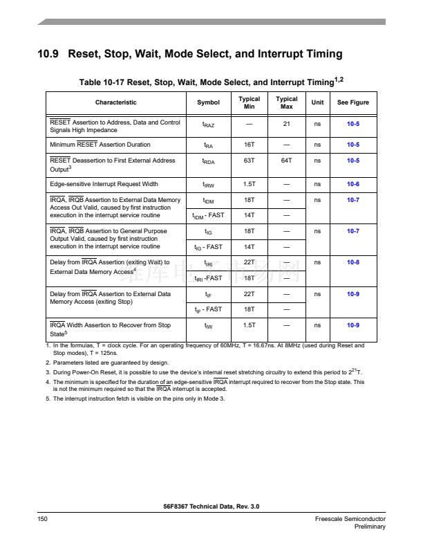 150
150
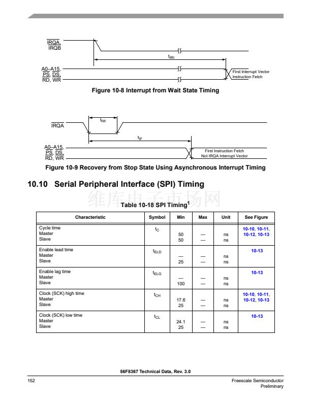
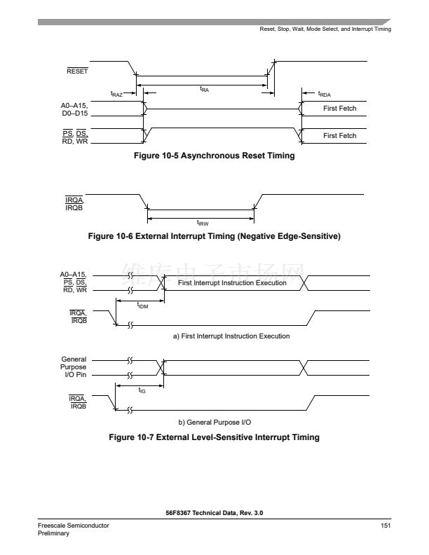 151
151
 152
152
 153
153
 154
154
 155
155
 156
156
 157
157
 158
158
 159
159
 160
160
 161
161
 162
162
 163
163
 164
164
 165
165
 166
166
 167
167
 168
168
 169
169
 170
170
 171
171
 172
172
 173
173
 174
174
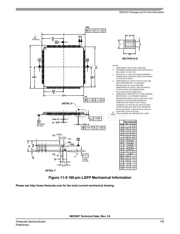 175
175
 176
176
 177
177
 178
178
 179
179
 180
180
