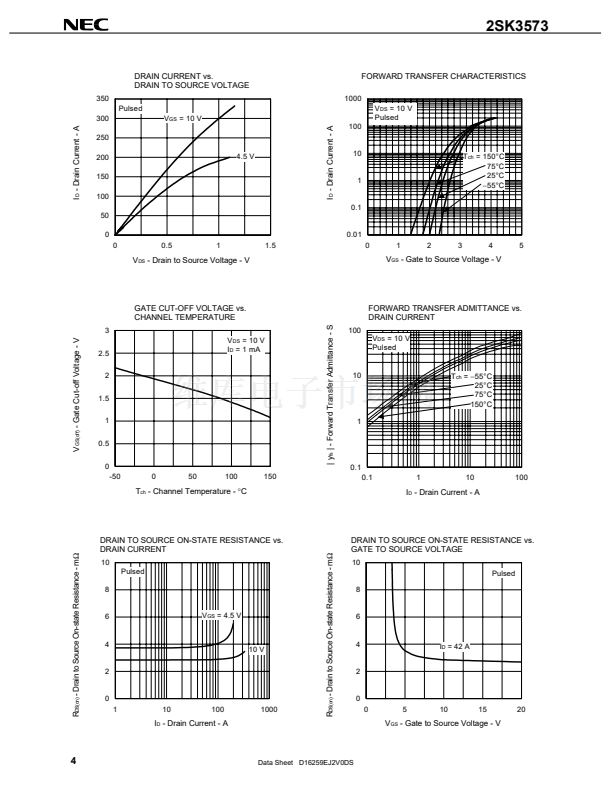
2SK3573
5
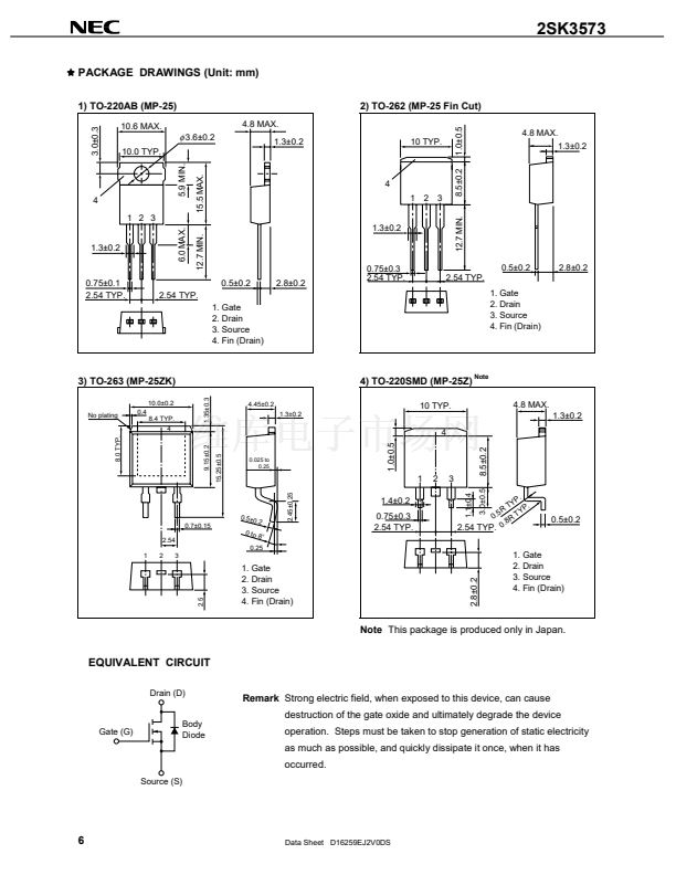
PACKAGE DRAWINGS (Unit: mm)
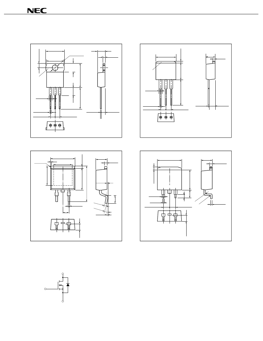
1) TO-220AB (MP-25)
3.0卤0.3
10.6 MAX.
10.0 TYP.
4.8 MAX.
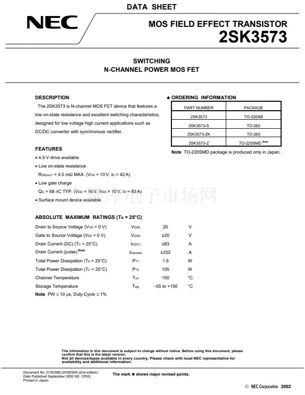
2) TO-262 (MP-25 Fin Cut)
1.0卤0.5
蠁
3.6卤0.2
5.9 MIN.
4.8 MAX.
1.3卤0.2
1.3卤0.2
10 TYP.
15.5 MAX.
4
1
2
3
4
1 2 3
6.0 MAX.
1.3卤0.2
1.3卤0.2
12.7 MIN.
12.7 MIN.
8.5卤0.2
0.75卤0.1
2.54 TYP.
0.5卤0.2
2.54 TYP.
1. Gate
2. Drain
3. Source
4. Fin (Drain)
2.8卤0.2
0.75卤0.3
2.54 TYP.
0.5卤0.2
2.54 TYP.
1. Gate
2. Drain
3. Source
4. Fin (Drain)
2.8卤0.2
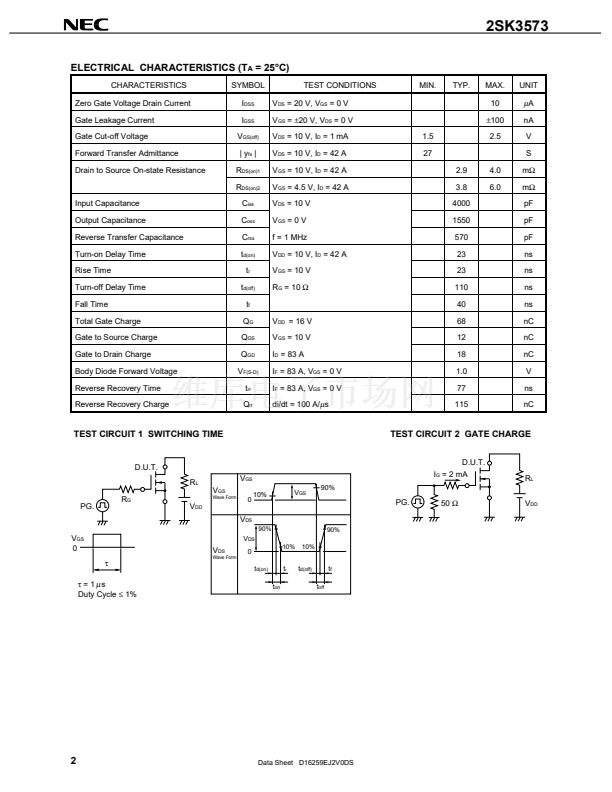
3) TO-263 (MP-25ZK)
10.0卤0.2
No plating
0.4
8.4 TYP.
4
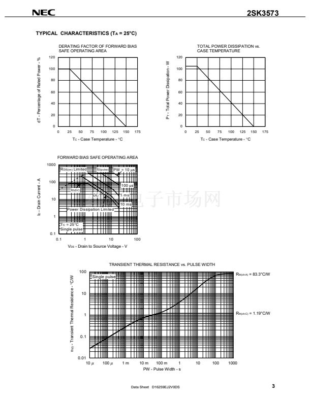
4) TO-220SMD (MP-25Z)
1.35卤0.3
4.45卤0.2
1.3卤0.2
Note
10 TYP.
4
4.8 MAX.
1.3卤0.2
8.0 TYP.
1.0卤0.5
9.15卤0.2
15.25卤0.5
0.025 to
0.25
1
2.45卤0.25
2
3
1.1卤0.4
3.0卤0.5
8.5卤0.2
P.
TY
P.
R
Y
0.5
R T
8
0.
1.4卤0.2
0.75卤0.3
2.54 TYP.
0.7卤0.15
2.54
1
2
3
0.5卤
0.2
0 to
8
o
2.54 TYP.
0.5卤0.2
0.25
Note
This package is produced only in Japan.
EQUIVALENT CIRCUIT
Drain (D)
Remark
Strong electric field, when exposed to this device, can cause
destruction of the gate oxide and ultimately degrade the device
operation. Steps must be taken to stop generation of static electricity
as much as possible, and quickly dissipate it once, when it has
occurred.
Gate (G)
Body
Diode
Source (S)
6
Data Sheet D16259EJ2V0DS
2.8卤0.2
2.5
1. Gate
2. Drain
3. Source
4. Fin (Drain)
1. Gate
2. Drain
3. Source
4. Fin (Drain)


 1
1
 2
2
 3
3
 4
4
 5
5
 6
6
 7
7
 8
8
