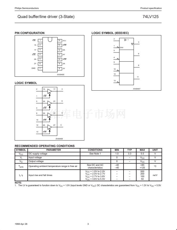
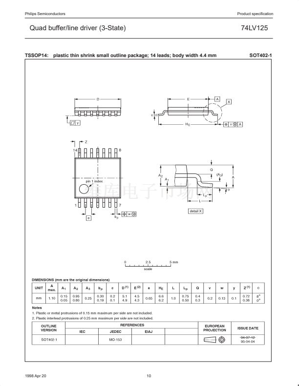
鈮?/div>
2.5 ns
SYMBOL
t
PHL
/t
PLH
C
I
C
PD
PARAMETER
Propagation delay
nA to nY
Input capacitance
Power dissipation capacitance per buffer
T
amb
= 25掳C.
T
amb
= 25掳C.
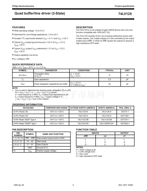
DESCRIPTION
The 74LV125 is a low-voltage Si-gate CMOS device and is pin and
function compatible with 74HC/HCT125.
The 74LV125 consists of four non-inverting buffers/line drivers with
3-state outputs. The 3-state outputs (nY) are controlled by the output
enable input (nOE). A HIGH at nOE causes the outputs to assume a
high impedance OFF-state.
CONDITIONS
C
L
= 15 pF;
V
CC
= 3.3 V
V
CC
= 3.3 V;
V
I
= GND to V
CC1
TYPICAL
9
3.5
22
UNIT
ns
pF
pF
NOTE:
1. C
PD
is used to determine the dynamic power dissipation (P
D
in
碌W)
P
D
= C
PD
脳
V
CC2
脳
f
i
)
(C
L
脳
V
CC2
脳
f
o
) where:
f
i
= input frequency in MHz; C
L
= output load capacitance in pF;
f
o
= output frequency in MHz; V
CC
= supply voltage in V;
(C
L
脳
V
CC2
脳
f
o
) = sum of the outputs.
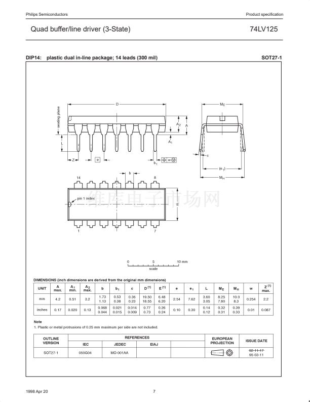
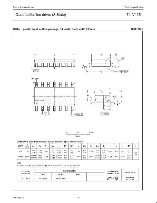
ORDERING INFORMATION
PACKAGES
14-Pin Plastic DIL
14-Pin Plastic SO
14-Pin Plastic SSOP Type II
14-Pin Plastic TSSOP Type I
TEMPERATURE RANGE
鈥?0掳C to +125掳C
鈥?0掳C to +125掳C
鈥?0掳C to +125掳C
鈥?0掳C to +125掳C
OUTSIDE NORTH AMERICA
74LV125 N
74LV125 D
74LV125 DB
74LV125 PW
NORTH AMERICA
74LV125 N
74LV125 D
74LV125 DB
74LV125PW DH
PKG. DWG. #
SOT27-1
SOT108-1
SOT337-1
SOT402-1
PIN DESCRIPTION
PIN
NUMBER
1, 4, 10, 13
2, 5, 9, 12
3, 6, 8, 11
7
14
SYMBOL
1OE 鈥?4OE
1A 鈥?4A
1Y 鈥?4Y
GND
V
CC
NAME AND FUNCTION
FUNCTION TABLE
INPUTS
nOE
Data enable inputs (active LOW)
Data inputs
Data Outputs
Ground (0 V)
Positive supply voltage
L
L
H
NOTES:
H = HIGH voltage level
L = LOW voltage level
X = don鈥檛 care
Z = high impedance OFF-state
nA
L
H
X
OUTPUT
nY
L
H
Z
1998 Apr 28
2
853鈥?901 19290


 1
1
 2
2
 3
3
 4
4
 5
5
 6
6
 7
7
 8
8
 9
9
 10
10
 11
11
 12
12
