Philips Semiconductors
Product specification
Quad buffer/line driver (3-State)
74LV125
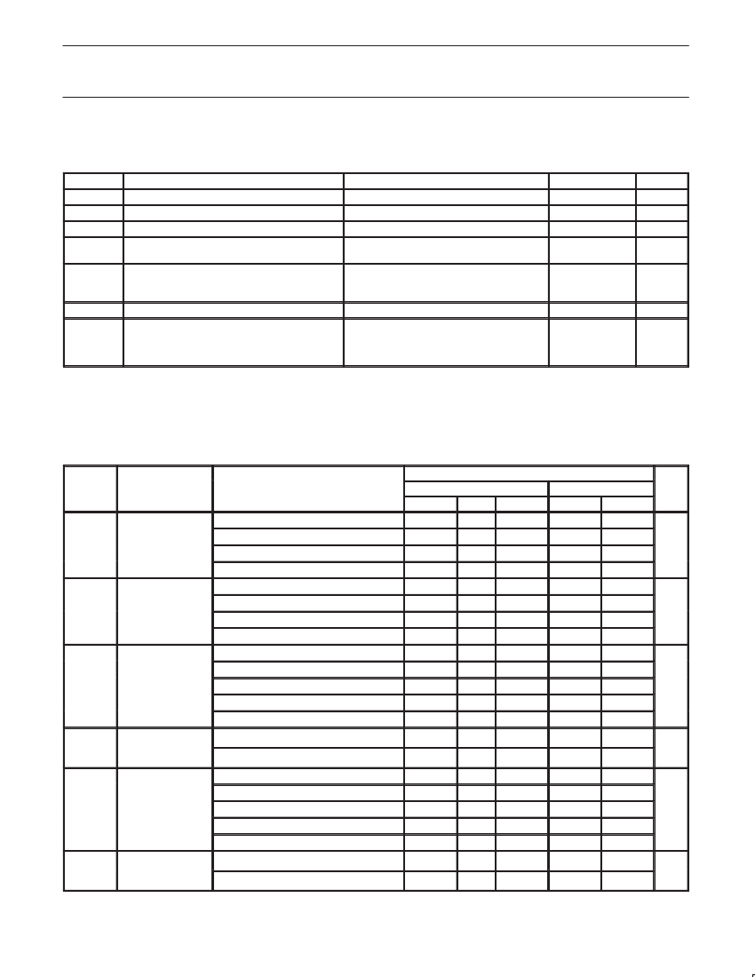
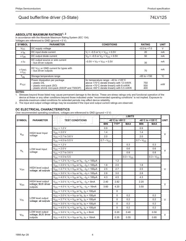
ABSOLUTE MAXIMUM RATINGS
1, 2
In accordance with the Absolute Maximum Rating System (IEC 134).
Voltages are referenced to GND (ground = 0 V).
SYMBOL
V
CC
"I
IK
"I
OK
"I
O
"I
GND
,
"I
CC
T
stg
P
TOT
PARAMETER
DC supply voltage
DC input diode current
DC output diode current
DC output source or sink current
鈥?bus driver outputs
DC V
CC
or GND current for types with
鈥?bus driver outputs
Storage temperature range
Power dissipation per package
鈥?plastic DIL
鈥?plastic mini-pack (SO)
鈥?plastic shrink mini-pack (SSOP and TSSOP)
for temperature range: 鈥?0 to +125掳C
above +70掳C derate linearly with 12 mW/K
above +70掳C derate linearly with 8 mW/K
above +60掳C derate linearly with 5.5 mW/K
V
I
< 鈥?.5 or V
I
> V
CC
+ 0.5V
V
O
< 鈥?.5 or V
O
> V
CC
+ 0.5V
鈥?.5V < V
O
< V
CC
+ 0.5V
CONDITIONS
RATING
鈥?.5 to +7.0
20
50
35
70
鈥?5 to +150
750
500
400
UNIT
V
mA
mA
mA
mA
掳C
mW
NOTES:
1. Stresses beyond those listed may cause permanent damage to the device. These are stress ratings only and functional operation of the
device at these or any other conditions beyond those indicated under 鈥渞ecommended operating conditions鈥?is not implied. Exposure to
absolute-maximum-rated conditions for extended periods may affect device reliability.
2. The input and output voltage ratings may be exceeded if the input and output current ratings are observed.
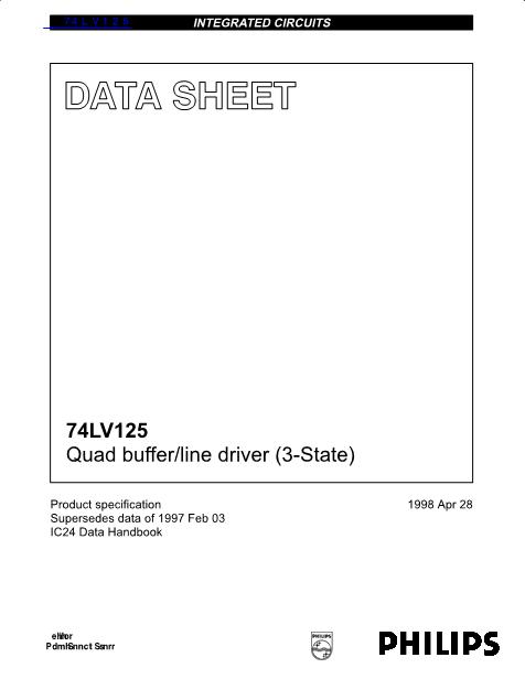
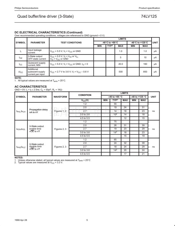
DC ELECTRICAL CHARACTERISTICS
Over recommended operating conditions, voltages are referenced to GND (ground = 0 V)
LIMITS
SYMBOL
PARAMETER
TEST CONDITIONS
MIN
V
CC
= 1.2 V
V
IH
HIGH level Input
voltage
V
CC
= 2.0 V
V
CC
= 2.7 to 3.6 V
V
CC
= 4.5 to 5.5 V
V
CC
= 1.2 V
V
IL
LOW level Input
voltage
V
CC
= 2.0 V
V
CC
= 2.7 to 3.6 V
V
CC
= 4.5 to 5.5
V
CC
= 1.2 V; V
I
= V
IH
or V
IL;
鈥揑
O
= 100碌A
V
CC
= 2.0 V; V
I
= V
IH
or V
IL;
鈥揑
O
= 100碌A
V
OH
HIGH l
level output
l t t
voltage
out uts
voltage; all outputs
V
CC
= 2.7 V; V
I
= V
IH
or V
IL;
鈥揑
O
= 100碌A
V
CC
= 3.0 V; V
I
= V
IH
or V
IL;
鈥揑
O
= 100碌A
V
CC
= 4.5 V; V
I
= V
IH
or V
IL;
鈥揑
O
= 100碌A
V
OH
HIGH level output
voltage; BUS driver
outputs
V
CC
= 3.0 V; V
I
= V
IH
or V
IL;
鈥揑
O
= 8mA
V
CC
= 4.5 V; V
I
= V
IH
or V
IL;
鈥揑
O
= 16mA
V
CC
= 1.2 V; V
I
= V
IH
or V
IL;
I
O
= 100碌A
V
CC
= 2.0 V; V
I
= V
IH
or V
IL;
I
O
= 100碌A
V
OL
LOW l
level output
l t t
voltage
out uts
voltage; all outputs
V
CC
= 2.7 V; V
I
= V
IH
or V
IL;
I
O
= 100碌A
V
CC
= 3.0 V; V
I
= V
IH
or V
IL;
I
O
= 100碌A
V
CC
= 4.5 V; V
I
= V
IH
or V
IL;
I
O
= 100碌A
V
OL
LOW level output
voltage; BUS driver
outputs
V
CC
= 3.0 V; V
I
= V
IH
or V
IL;
I
O
= 8mA
V
CC
= 4.5 V; V
I
= V
IH
or V
IL;
I
O
= 16mA
1.8
2.5
2.8
4.3
2.40
3.60
1.2
2.0
2.7
3.0
4.5
2.82
4.20
0
0
0
0
0
0.20
0.35
0.2
0.2
0.2
0.2
0.40
0.55
0.2
0.2
0.2
0.2
0.50
V
0.65
V
1.8
2.5
2.8
4.3
2.20
V
3.50
V
0.9
1.4
2.0
0.7<V
CC
0.3
0.6
0.8
0.3<V
CC
-40掳C to +85掳C
TYP
1
MAX
-40掳C to +125掳C
MIN
0.9
1.4
2.0
0.7<V
CC
0.3
0.6
0.8
0.3<V
CC
V
V
MAX
UNIT
1998 Apr 28
4


 1
1
 2
2
 3
3
 4
4
 5
5
 6
6
 7
7
 8
8
 9
9
 10
10
 11
11
 12
12
