鈥?/div>
Positive-edge triggered clock
DESCRIPTION
The 74LVC169 is a high-performance, low-power, low-voltage,
Si-gate CMOS device and superior to most advanced CMOS
compatible TTL families.
The 74LVC169 is a synchronous presettable binary counter which
features an internal lookahead carry and can be used for high-speed
counting. Synchronous operation is provided by having all flip-flops
clocked simultaneously on the positive-going edge of the clock (CP).
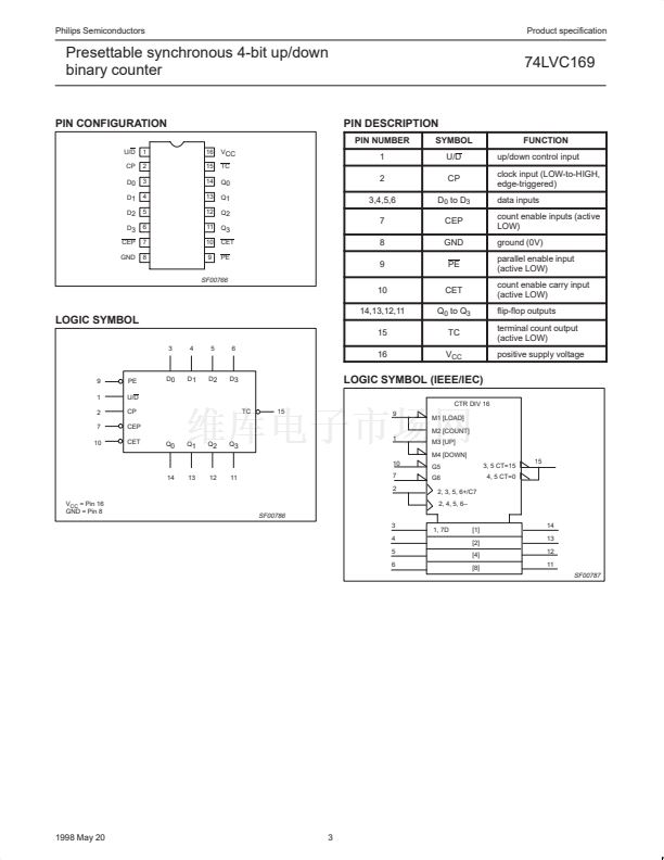
The outputs (Q
0
to Q
3
) of the counters may be preset to a HIGH or
LOW level. A LOW level at the parallel enable input (PE) disables
the counting action and causes the data at the data inputs
(D
0
to D
3
) to be loaded into the counter on the positive-going edge
of the clock (provided that the set-up and hold time requirements for
PE are met). Preset takes place regardless of the levels at count
enable inputs (CEP and CET). A low level at the master reset input
(MR) sets all four outputs of the flip-flops (Q
0
to Q
3
) to LOW level
after the next positive-going transition on the clock (CP) input
(provided that the set-up and hold time requirements for PE are
met).
This action occurs regardless of the levels at CP, PE, CET and CEP
inputs This synchronous reset feature enables the designer to
modify the maximum count with only one external NAND gate.
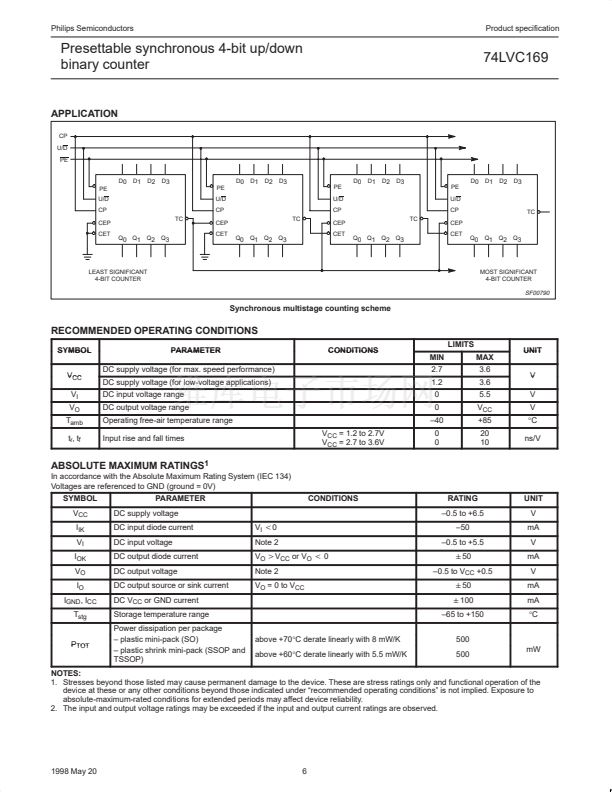
The lookahead carry simplifies serial cascading of the counters.
Both count enable inputs (CEP and CET) must be HIGH to count.
The CET input is fed forward to enable the terminal count output
(TC). The TC output thus enabled will produce a HIGH output pulse
of a duration approximately equal to a HIGH level output of Q
0
. This
pulse can be used to enable the next cascaded stage. The
maximum clock frequency for the cascaded counters is determined
by the CP to TC propagation delay and CEP to CP set-up time,
according to the following formula:
1
f
max
= _______________________________
tp
(max)
(CP to TC) + t
SU
(CEP to CP)
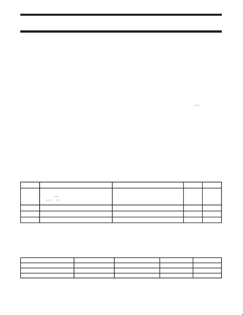
QUICK REFERENCE DATA
GND = 0V; T
amb
= 25掳C; T
R
= T
F
�
2.5ns
SYMBOL
PARAMETER
Propagation delay
CP to Q
n
CP to TC
CET to TC
maximum clock frequency
input capacitance
power dissipation capacitance per gate
notes 1 and 2
CONDITIONS
C
L
= 50 pF
V
CC
= 3.3V
TYPICAL
5.0
6.5
5.3
200
5.0
42
UNIT
t
PHL
/t
PLH
ns
f
MAX
C
I
C
PD
MHz
pF
pF
NOTES:
1. C
PD
is used to determine the dynamic power dissipation (P
D
in
碌W)
P
D
= C
PD
x V
CC2
x f
i
+危 (C
L
x V
CC2
x f
o )
where:
f
i
= input frequency in MHz; C
L
= output load capacity in pF;
f
o
= output frequency in MHz; V
CC
= supply voltage in V;
危
(C
L
x V
CC2
x f
o )
= sum of the outputs
2. The condition is V
1
= GND to V
CC
ORDERING INFORMATION
PACKAGES
16-Pin Plastic SO
16-Pin Plastic SSOP Type II
16-Pin Plastic TSSOP Type I
TEMPERATURE RANGE
鈥?0掳C to +85掳C
鈥?0掳C to +85掳C
鈥?0掳C to +85掳C
OUTSIDE NORTH AMERICA
74LVC169 D
74LVC169 DB
74LVC169 PW
NORTH AMERICA
74LVC169 D
74LVC169 DB
74LVC169PW DH
DWG NUMBER
SOT109-1
SOT338-1
SOT403-1
1998 May 20
2
853-1866 19421


 1
1
 2
2
 3
3
 4
4
 5
5
 6
6
 7
7
 8
8
 9
9
 10
10
 11
11
 12
12
 13
13
 14
14
