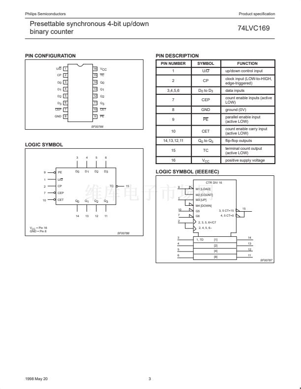
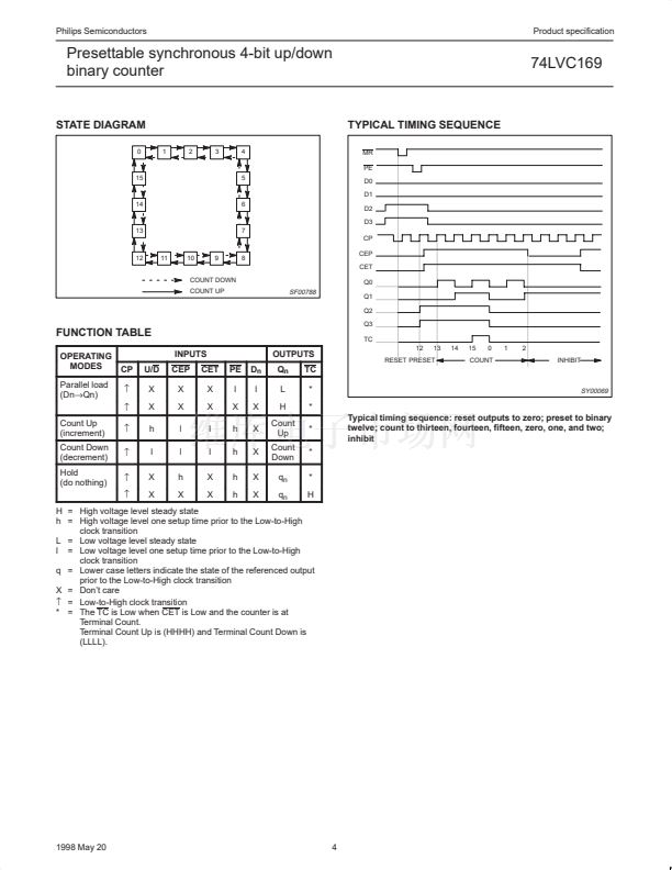
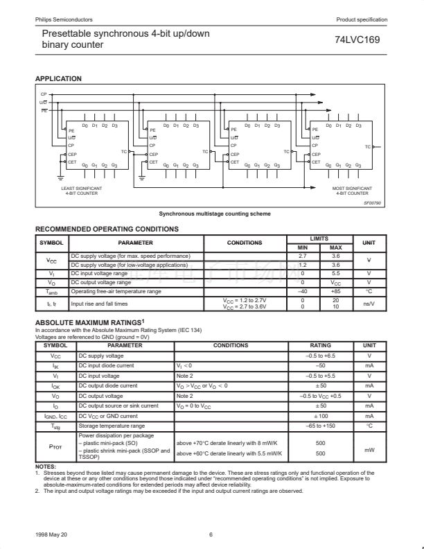
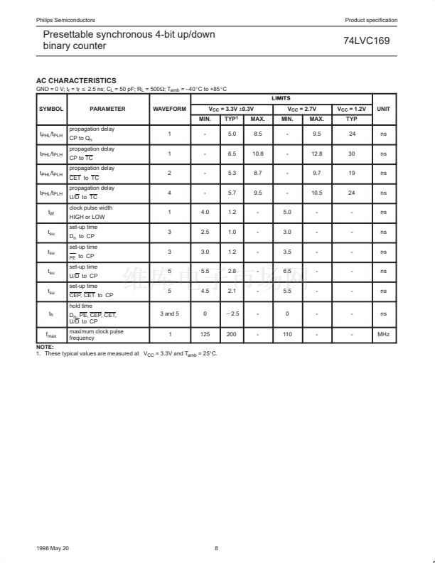
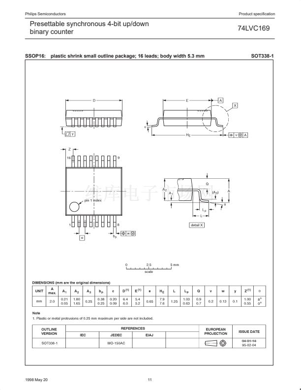
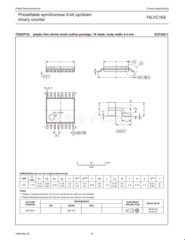
Philips Semiconductors
Product specification
Presettable synchronous 4-bit up/down
binary counter
74LVC169
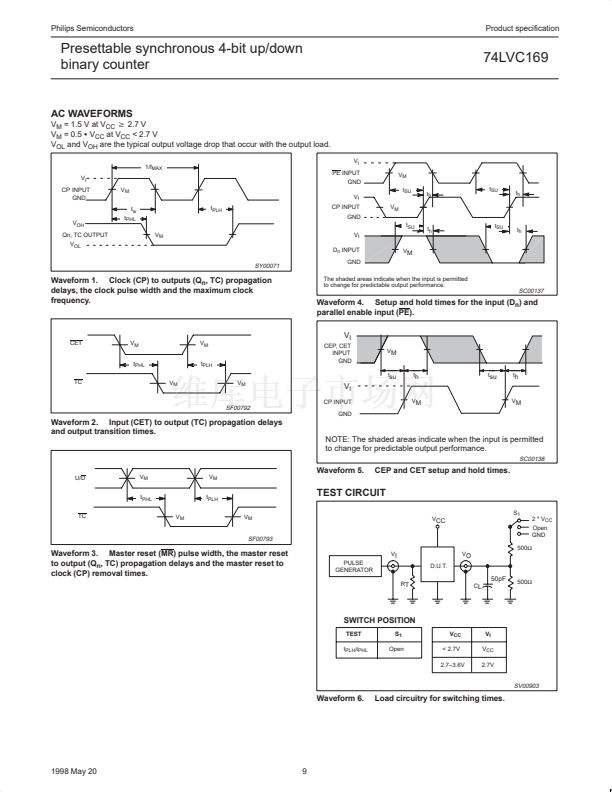
AC WAVEFORMS
V
M
= 1.5 V at V
CC
w
2.7 V
V
M
= 0.5
S
V
CC
at V
CC
< 2.7 V
V
OL
and V
OH
are the typical output voltage drop that occur with the output load.
1/f
MAX
V
I
CP INPUT
GND
V
M
V
I
t
w
V
OH
Qn, TC OUTPUT
V
OL
t
PHL
V
M
t
PLH
CP INPUT
GND
t
SU
V
I
D
n
INPUT
V
M
t
h
t
SU
t
h
V
M
V
I
PE INPUT
GND
V
M
t
SU
t
h
t
SU
t
h
SY00071
GND
The shaded areas indicate when the input is permitted
to change for predictable output performance.
Waveform 1. Clock (CP) to outputs (Q
n
, TC) propagation
delays, the clock pulse width and the maximum clock
frequency.
SC00137
Waveform 4. Setup and hold times for the input (D
n
) and
parallel enable input (PE).
V
I
CET
V
M
t
PHL
V
M
t
PLH
V
M
V
M
CEP, CET
INPUT
GND
V
M
TC
t
su
t
h
t
su
t
h
V
I
CP INPUT
V
M
V
M
GND
SF00792
Waveform 2. Input (CET) to output (TC) propagation delays
and output transition times.
NOTE: The shaded areas indicate when the input is permitted
to change for predictable output performance.
SC00138
Waveform 5.
U/D
V
M
t
PHL
TC
V
M
V
M
t
PLH
V
M
CEP and CET setup and hold times.
TEST CIRCUIT
V
CC
S
1
2 * V
CC
Open
GND
SF00793
Waveform 3. Master reset (MR) pulse width, the master reset
to output (Q
n
, TC) propagation delays and the master reset to
clock (CP) removal times.
500鈩?/div>
V
I
PULSE
GENERATOR
R
T
D.U.T.
V
O
50pF
C
L
500鈩?/div>
SWITCH POSITION
TEST
t
PLH/
t
PHL
S
1
Open
V
CC
< 2.7V
2.7鈥?.6V
V
I
V
CC
2.7V
SV00903
Waveform 6.
Load circuitry for switching times.
1998 May 20
9


 1
1
 2
2
 3
3
 4
4
 5
5
 6
6
 7
7
 8
8
 9
9
 10
10
 11
11
 12
12
 13
13
 14
14
