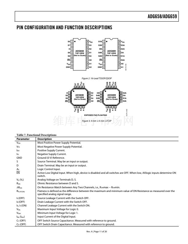
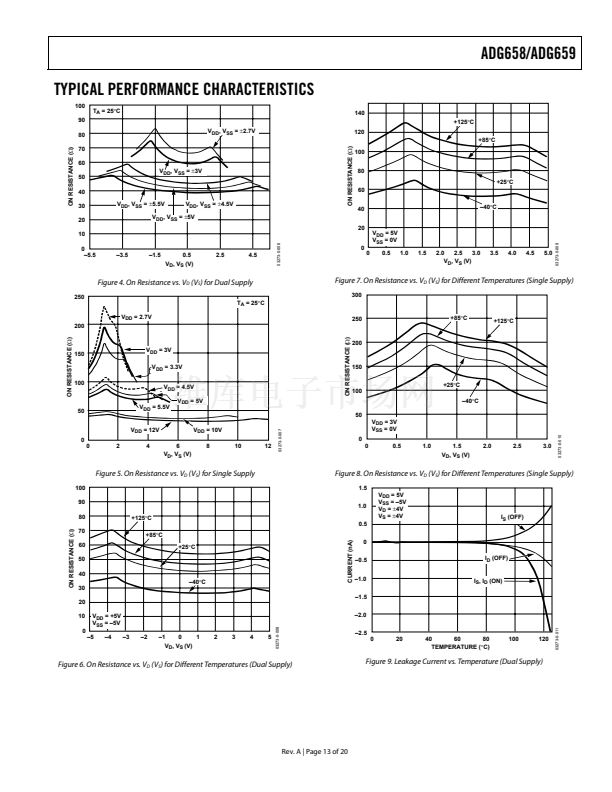
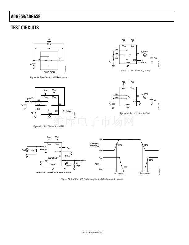
ADG658/ADG659
Parameter
C
D
, C
S
(ON)
C
IN
t
ON
t
OFF
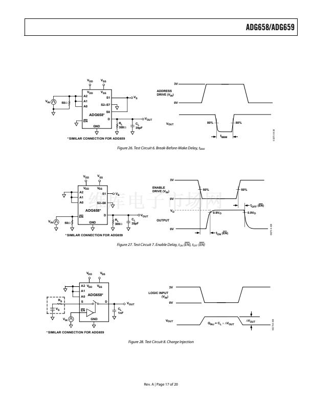
t
BBM
Charge
Injection
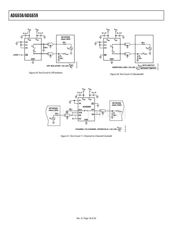
Off Isolation
Crosstalk
Bandwidth
On Response
Insertion Loss
Description
ON Switch Capacitance. Measured with reference to ground.
Digital Input Capacitance.
Delay between Applying the Digital Control Input and the Output Switching ON. See Test Circuit 7.
Delay between Applying the Digital Control Input and the Output Switching OFF.
ON Time. Measured between 80% points of both switches when switching from one address state to another.
Measure of the Glitch Impulse Transferred from the Digital Input to the Analog Output during Switching.
Measure of Unwanted Signal Coupling through an OFF Switch.
Measure of Unwanted Signal Coupled through from One Channel to Another as a Result of Parasitic Capacitance.
The Frequency at which the Output is Attenuated by 3 dB.
The Frequency Response of the ON Switch.
The Loss Due to the ON Resistance of the Switch.
Rev. A | Page 12 of 20


 1
1
 2
2
 3
3
 4
4
 5
5
 6
6
 7
7
 8
8
 9
9
 10
10
 11
11
 12
12
 13
13
 14
14
 15
15
 16
16
 17
17
 18
18
 19
19
 20
20
