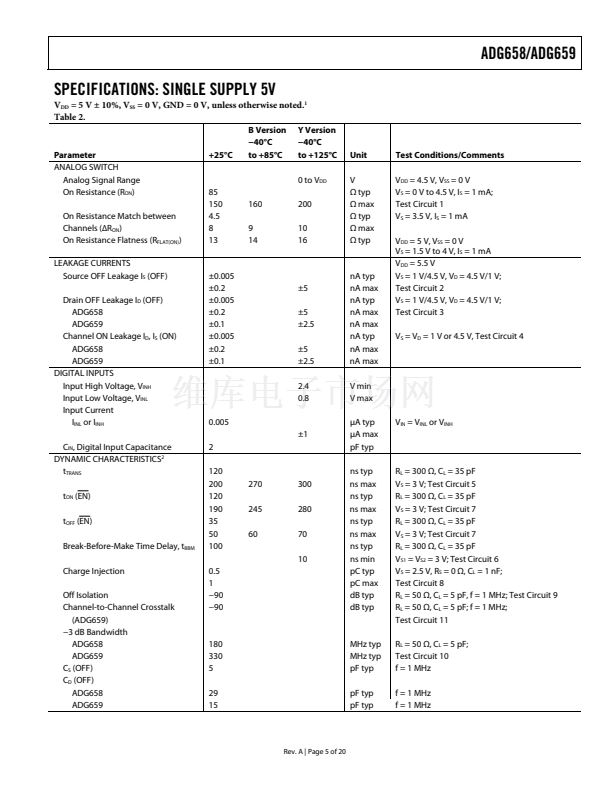
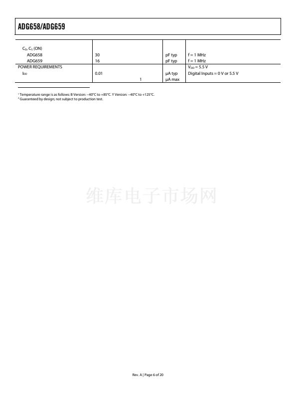
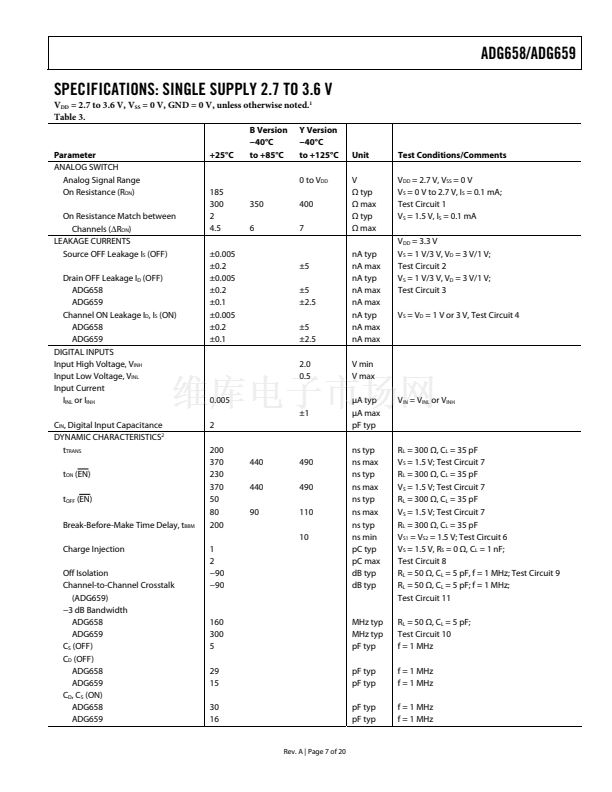
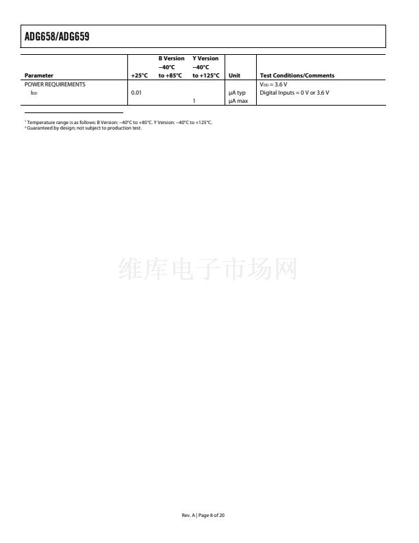
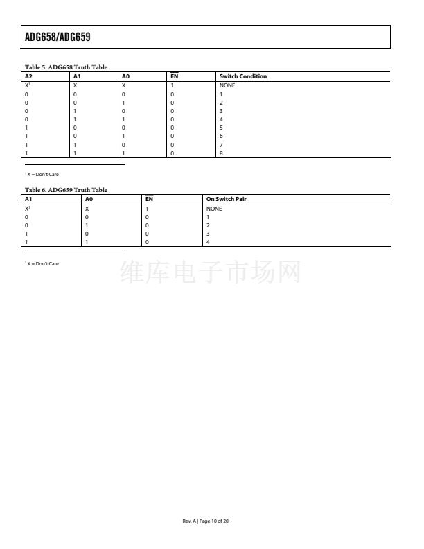
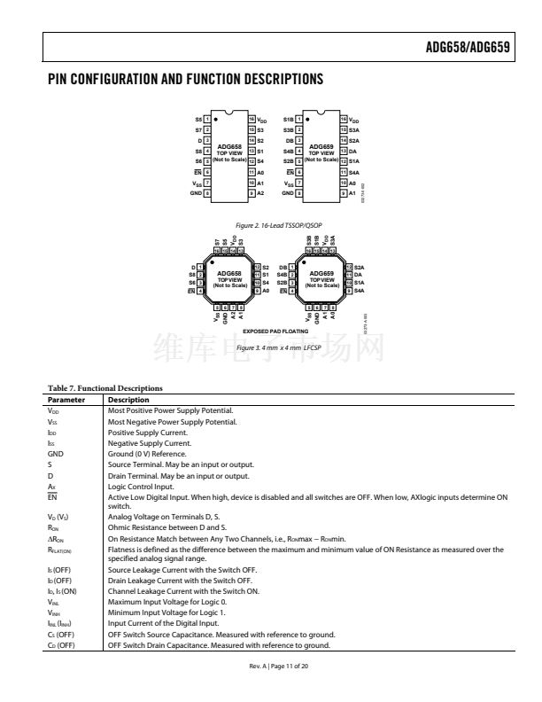
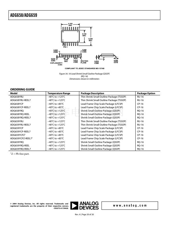
ADG658/ADG659
ABSOLUTE MAXIMUM RATINGS
TA = 25掳C, unless otherwise noted.
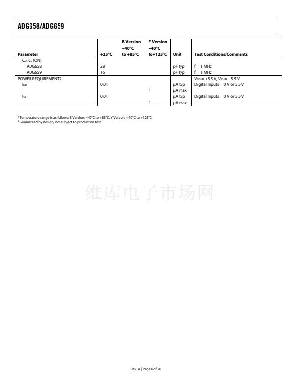
Table 4.
Parameters
V
DD
to V
SS
V
DD
to GND
V
SS
to GND
Analog Inputs
1
Digital Inputs
1
Ratings
13 V
鈭?.3 V to +13 V
+0.3 V to 鈭?.5 V
V
SS
鈭?.3 V to V
DD
+0.3 V
GND 鈭?.3 V to V
DD
+0.3
V or 10 mA, whichever
occurs first
40 mA
20 mA
鈭?0掳C to +125掳C
鈭?0掳C to +85掳C
鈭?5掳C to +150掳C
150掳C
104掳C/W
150.4掳C/W
Stresses above those listed under Absolute Maximum Ratings
may cause permanent damage to the device. This is a stress
rating only; functional operation of the device at these or any
other conditions above those indicated in the operational
section of this specification is not implied. Exposure to absolute
maximum rating conditions for extended periods may affect
device reliability.
Peak Current, S or D
(Pulsed at 1 ms, 10% duty cycle max)
Continuous Current, S or D
Operating Temperature Range
Automotive (Y Version)
Industrial (B Version)
Storage Temperature Range
Junction Temperature
胃
JA
Thermal Impedance, 16-Lead
QSOP
胃
JA
Thermal Impedance, 16-Lead
TSSOP
胃
JA
Thermal Impedance (4-Layer
Board),
16-Lead LFCSP
Lead Temperature, Soldering
Vapor Phase (60 sec)
Infrared (15 sec)
ESD
70掳C/W
215掳C
220掳C
5.5 kV
1
Over voltages at A
X
, EN, S, or D are clamped by internal diodes. Current
should be limited to the maximum ratings.
ESD CAUTION
ESD (electrostatic discharge) sensitive device. Electrostatic charges as high as 4000 V readily accumulate on
the human body and test equipment and can discharge without detection. Although this product features
proprietary ESD protection circuitry, permanent damage may occur on devices subjected to high energy
electrostatic discharges. Therefore, proper ESD precautions are recommended to avoid performance
degradation or loss of functionality.
Rev. A | Page 9 of 20


 1
1
 2
2
 3
3
 4
4
 5
5
 6
6
 7
7
 8
8
 9
9
 10
10
 11
11
 12
12
 13
13
 14
14
 15
15
 16
16
 17
17
 18
18
 19
19
 20
20
