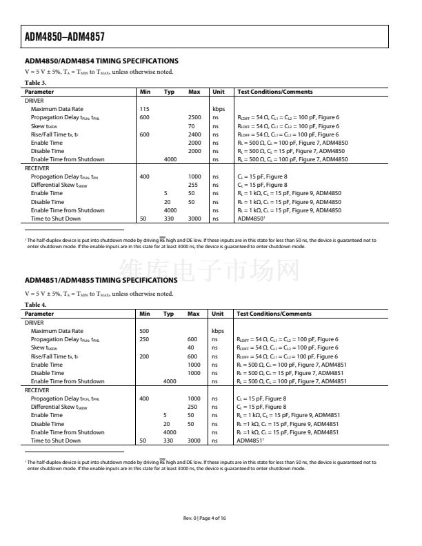
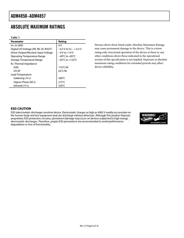
ADM4850鈥揂DM4857
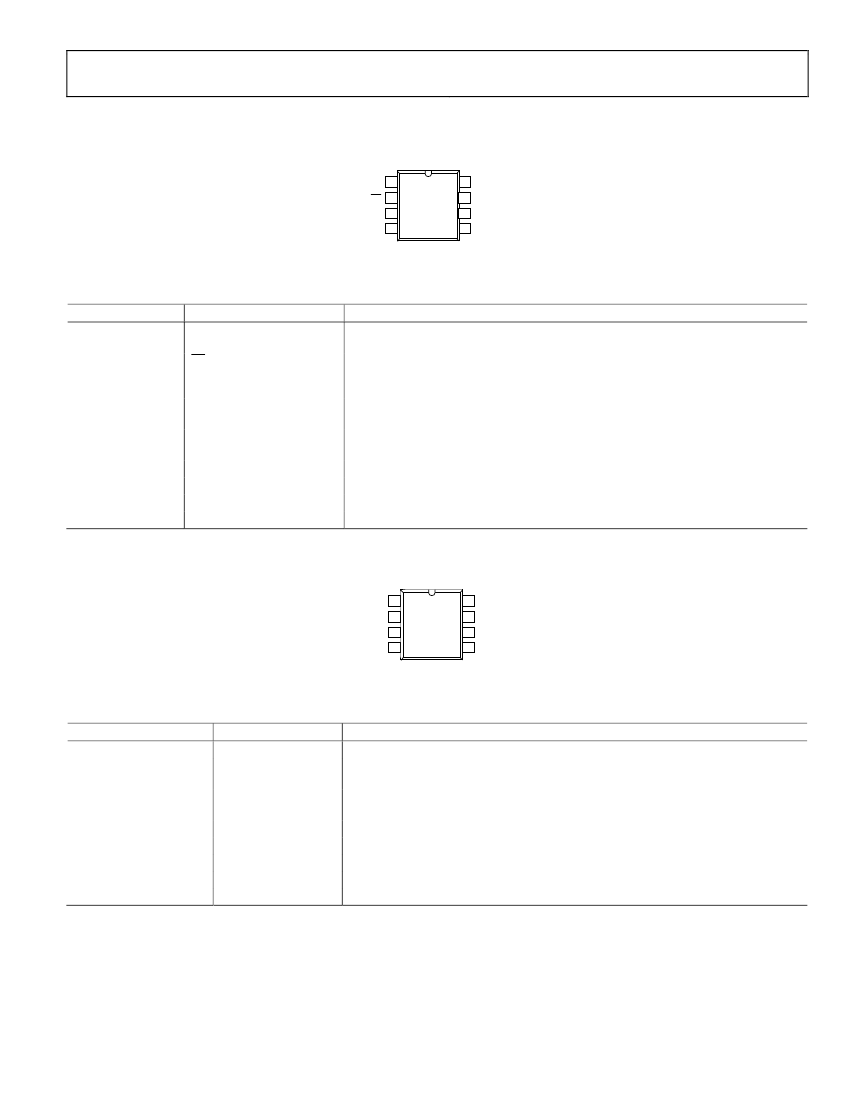
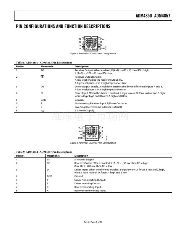
PIN CONFIGURATIONS AND FUNCTION DESCRIPTIONS
RO
1
RE
2
DE
3
Figure 2. ADM4850鈥揂DM4853 Pin Configuration
Table 8. ADM4850鈥揂DM4853 Pin Descriptions
Pin No.
1
2
Mnemonic
RO
RE
Description
Receiver Output. When enabled, if (A鈭払) 鈮?鈭?0 mV, then RO = high.
If (A鈭払) 鈮?鈭?00 mV, then RO = low.
Receiver Output Enable.
A low level enables the receiver output, RO.
A high level places it in a high impedance state.
Driver Output Enable. A high level enables the driver differential inputs A and B.
A low level places it in a high impedance state.
Driver Input. When the driver is enabled, a logic low on DI forces A low and B high,
while a logic high on DI forces A high and B low.
Ground.
Noninverting Receiver Input A/Driver Output A.
Inverting Receiver Input B/Driver Output B.
5 V Power Supply.
3
4
5
6
7
8
DE
DI
GND
A
B
V
CC
V
CC 1
RO
2
DI
3
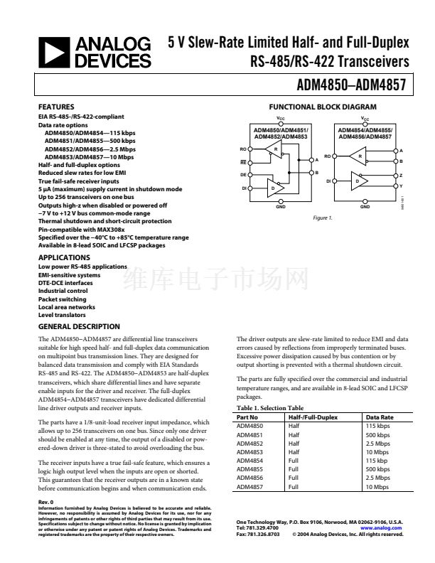
Figure 3. ADM4854鈥揂DM4857 Pin Configuration
Table 9. ADM4854鈥揂DM4857 Pin Descriptions
Pin No.
1
2
3
4
5
6
7
8
Mnemonic
V
CC
RO
DI
GND
Y
Z
B
A
Description
5 V Power Supply.
Receiver Output. When enabled, if (A鈭払) 鈮?鈭?0 mV, then RO = high.
If (A鈭払) 鈮?鈭?00 mV, then RO = low.
Driver Input. When the driver is enabled, a logic low on DI forces Y low and Z high,
while a logic high on DI forces Y high and Z low.
Ground.
Driver Noninverting Output.
Driver Inverting Output.
Receiver Inverting Input.
Receiver Noninverting Input.
Rev. 0 | Page 7 of 16
04931-003
6
Z
TOP VIEW
GND
4
(Not to Scale)
5
Y
ADM4854/
ADM4855/
ADM4856/
ADM4857
8
7
A
B
04931-002
A
TOP VIEW
DI
4
(Not to Scale)
5
GND
6
ADM4850/
ADM4851/
ADM4852/
ADM4853
8
7
V
CC
B


 1
1
 2
2
 3
3
 4
4
 5
5
 6
6
 7
7
 8
8
 9
9
 10
10
 11
11
 12
12
 13
13
 14
14
 15
15
 16
16
