www.ti.com
ADS5440
SLAS467 鈥?JULY 2005
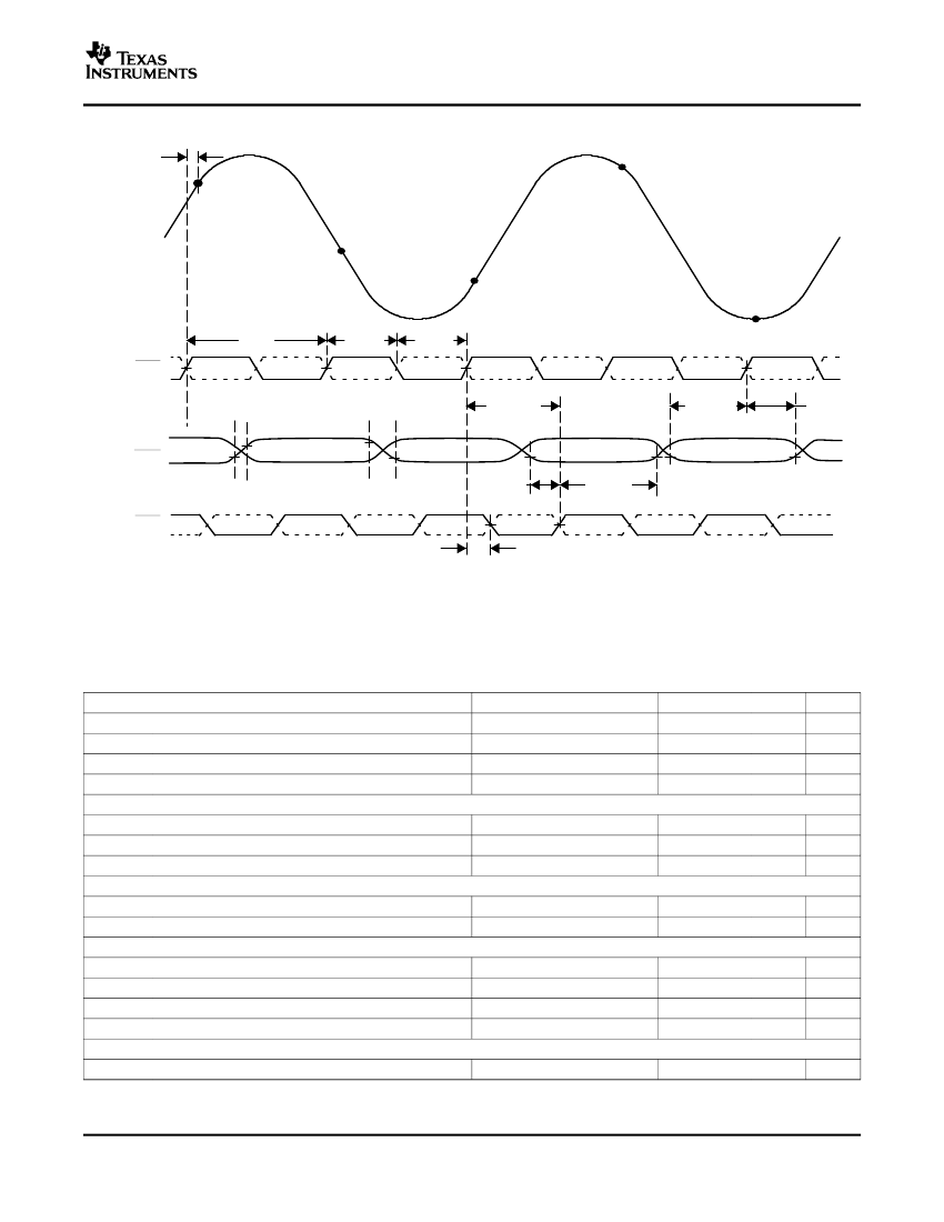
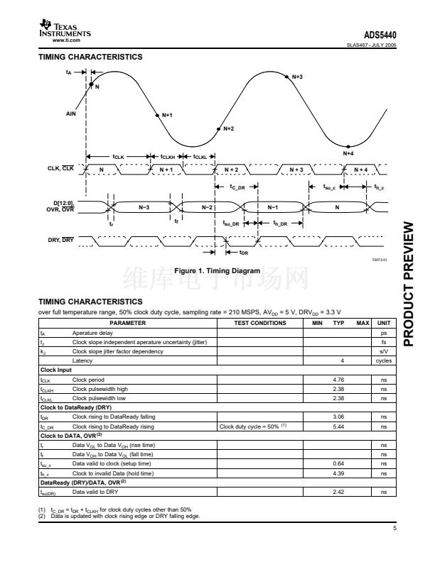
TIMING CHARACTERISTICS
t
A
N
N+3
AIN
N+1
N+2
t
CLK
CLK, CLK
N
t
CLKH
N+1
t
CLKL
N+2
t
C_DR
N+3
t
su_c
N+4
N+4
t
h_c
D[12:0],
OVR, OVR
t
r
DRY, DRY
N鈭?
t
f
N鈭?
t
su_DR
N鈭?
t
h_DR
N
t
DR
T0073-01
Figure 1. Timing Diagram
TIMING CHARACTERISTICS
over full temperature range, 50% clock duty cycle, sampling rate = 210 MSPS, AV
DD
= 5 V, DRV
DD
= 3.3 V
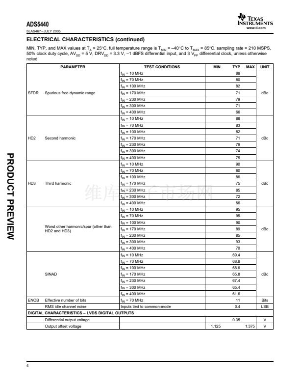
PARAMETER
t
A
t
J
k
J
Clock Input
t
CLK
t
CLKH
t
CLKL
t
DR
t
C_DR
t
r
t
f
t
su_c
t
h_c
t
su(DR)
(1)
(2)
Clock period
Clock pulsewidth high
Clock pulsewidth low
Clock rising to DataReady falling
Clock rising to DataReady rising
Data V
OL
to Data V
OH
(rise time)
Data V
OH
to Data V
OL
(fall time)
Data valid to clock (setup time)
Clock to invalid Data (hold time)
Data valid to DRY
0.64
4.39
2.42
Clock duty cycle = 50%
(1)
TEST CONDITIONS
MIN
TYP
MAX
UNIT
ps
fs
s/V
Aperature delay
Clock slope independent aperature uncertainty (jitter)
Clock slope jitter factor dependency
Latency
4
4.76
2.38
2.38
3.06
5.44
cycles
ns
ns
ns
ns
ns
ns
ns
ns
ns
ns
Clock to DataReady (DRY)
Clock to DATA, OVR
(2)
DataReady (DRY)/DATA, OVR
(2)
t
C_DR
= t
DR
+ t
CLKH
for clock duty cycles other than 50%
Data is updated with clock rising edge or DRY falling edge.
5
PRODUCT PREVIEW


 1
1
 2
2
 3
3
 4
4
 5
5
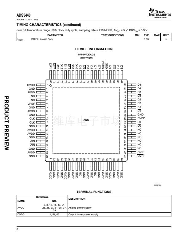 6
6
 7
7
 8
8
 9
9
 10
10
 11
11
