www.ti.com
ADS5440
SLAS467 鈥?JULY 2005
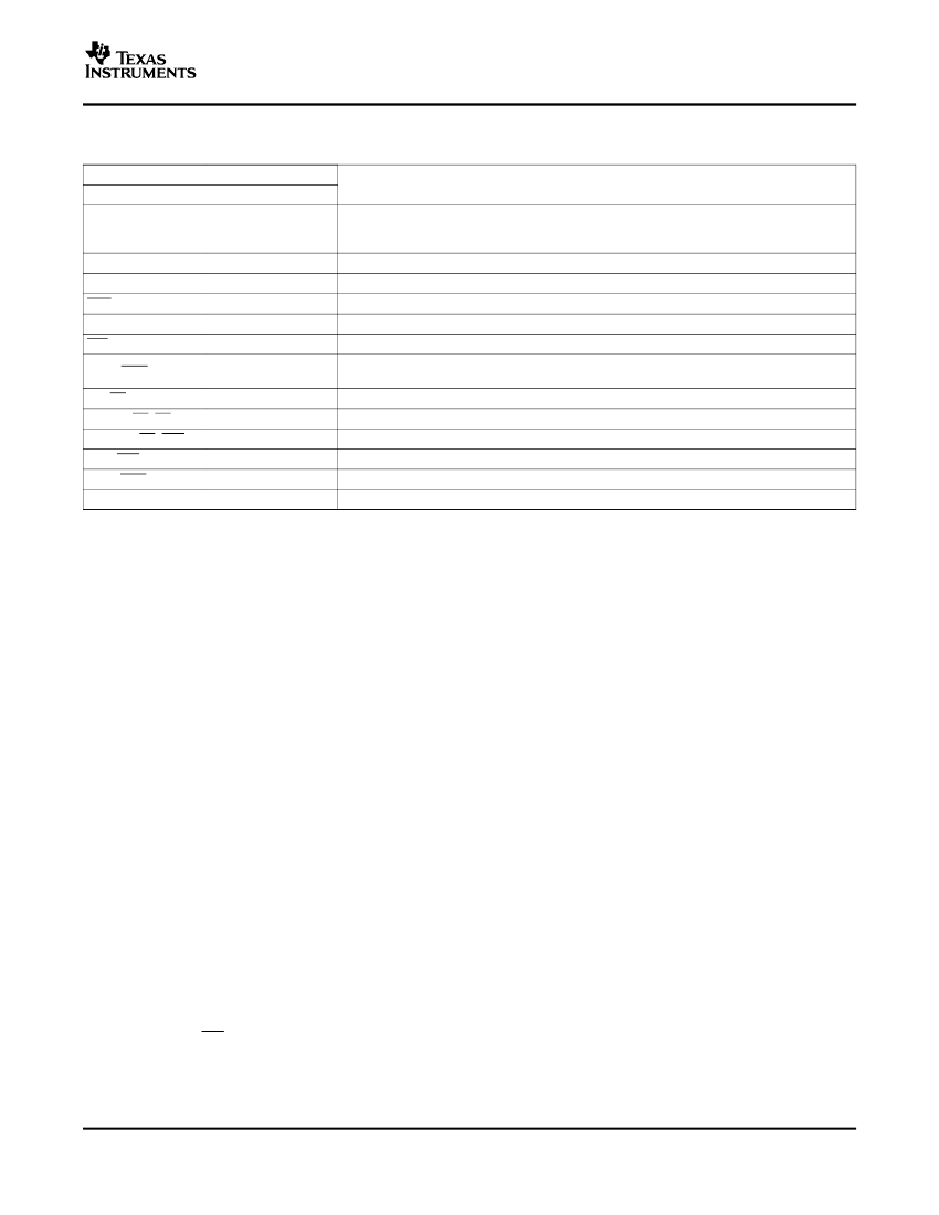
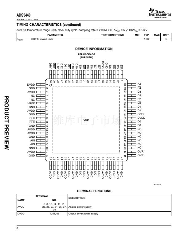
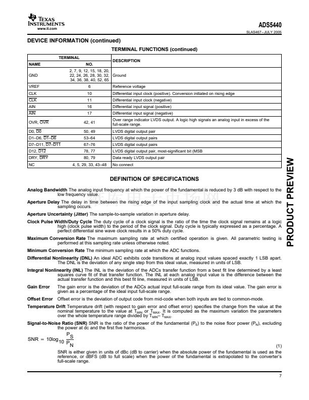
DEVICE INFORMATION (continued)
TERMINAL FUNCTIONS (continued)
TERMINAL
NAME
GND
VREF
CLK
CLK
AIN
AIN
OVR, OVR
D0, D0
D1鈥揇6, D1鈥揇6
D7鈥揇11, D7鈥揇11
D12, D12
DRY, DRY
NC
NO.
DESCRIPTION
2, 7, 9, 12, 15, 18, 20,
22, 24, 26, 28, 30, 32, Ground
34, 36, 38, 40, 52, 65
6
10
11
16
17
42, 41
50, 49
53鈥?4
67鈥?6
78, 77
80, 79
4, 5, 29, 33, 43鈥?8
Reference voltage
Differential input clock (positive). Conversion initiated on rising edge
Differential input clock (negative)
Differential input signal (positive)
Differential input signal (negative)
Over range indicator LVDS output. A logic high signals an analog input in excess of the
full-scale range.
LVDS digital output pair
LVDS digital output pairs
LVDS digital output pairs
LVDS digital output pair, most-significant bit (MSB
No connect
Data ready LVDS output pair
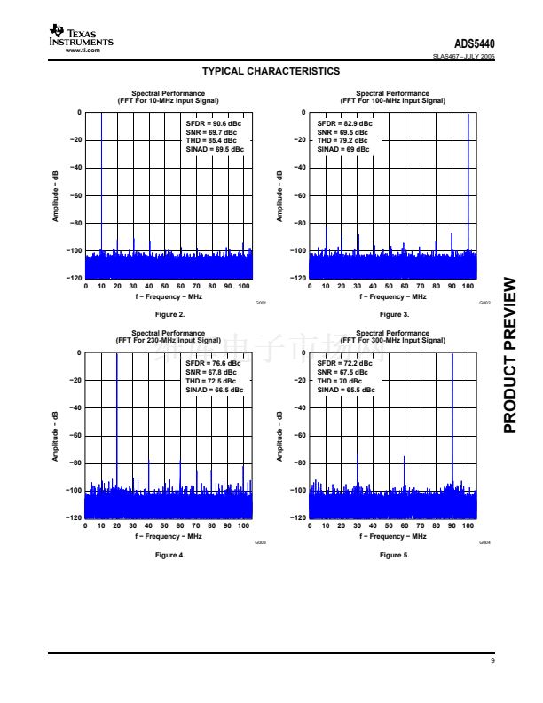
DEFINITION OF SPECIFICATIONS
Analog Bandwidth
The analog input frequency at which the power of the fundamental is reduced by 3 dB with respect to the
low frequency value.
Aperture Delay
The delay in time between the rising edge of the input sampling clock and the actual time at which the
sampling occurs.
Aperture Uncertainty (Jitter)
The sample-to-sample variation in aperture delay.
Clock Pulse Width/Duty Cycle
The duty cycle of a clock signal is the ratio of the time the clock signal remains at a logic
high (clock pulse width) to the period of the clock signal. Duty cycle is typically expressed as a percentage. A
perfect differential sine wave clock results in a 50% duty cycle.
Maximum Conversion Rate
The maximum sampling rate at which certified operation is given. All parametric testing is
performed at this sampling rate unless otherwise noted.
Minimum Conversion Rate
The minimum sampling rate at which the ADC functions.
Differential Nonlinearity (DNL)
An ideal ADC exhibits code transitions at analog input values spaced exactly 1 LSB apart.
The DNL is the deviation of any single step from this ideal value, measured in units of LSB.
Integral Nonlinearity (INL)
The INL is the deviation of the ADCs transfer function from a best fit line determined by a least
squares curve fit of that transfer function. The INL at each analog input value is the difference between the
actual transfer function and this best fit line, measured in units of LSB.
Gain Error
Offset Error
The gain error is the deviation of the ADCs actual input full-scale range from its ideal value. The gain error is
given as a percentage of the ideal input full-scale range.
Offset error is the deviation of output code from mid-code when both inputs are tied to common-mode.
Temperature Drift
Temperature drift (with respect to gain error and offset error) specifies the change from the value at the
nominal temperature to the value at T
MIN
or T
MAX
. It is computed as the maximum variation the parameters
over the whole temperature range divided by T
MIN
鈥?T
MAX
.
Signal-to-Noise Ratio (SNR)
SNR is the ratio of the power of the fundamental (P
S
) to the noise floor power (P
N
), excluding
the power at dc and the first five harmonics.
P
SNR
+
10log
10 P
S
N
(1)
SNR is either given in units of dBc (dB to carrier) when the absolute power of the fundamental is used as the
reference, or dBFS (dB to full scale) when the power of the fundamental is extrapolated to the converter鈥檚
full-scale range.
7
PRODUCT PREVIEW


 1
1
 2
2
 3
3
 4
4
 5
5
 6
6
 7
7
 8
8
 9
9
 10
10
 11
11
