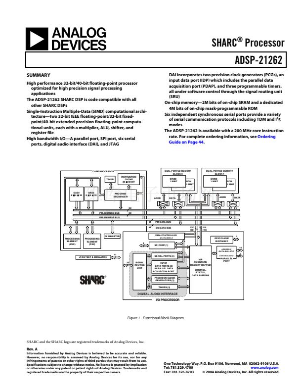
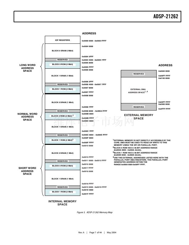
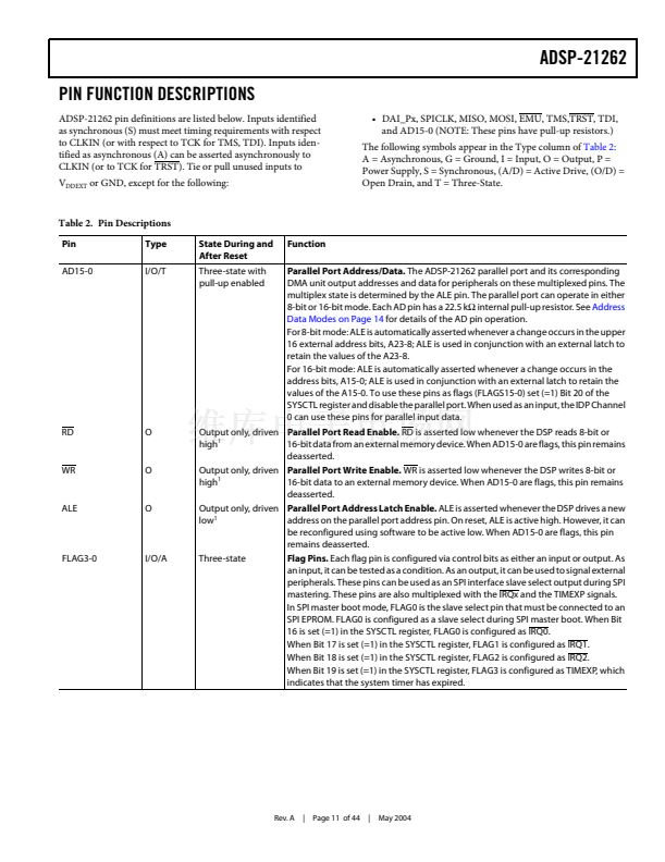
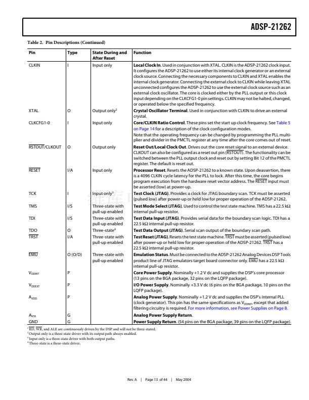
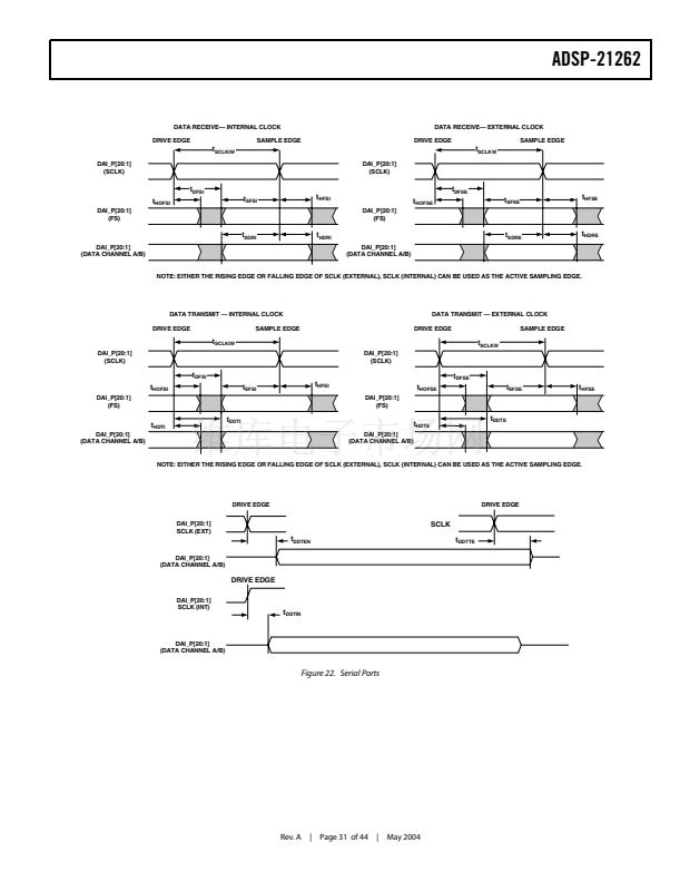
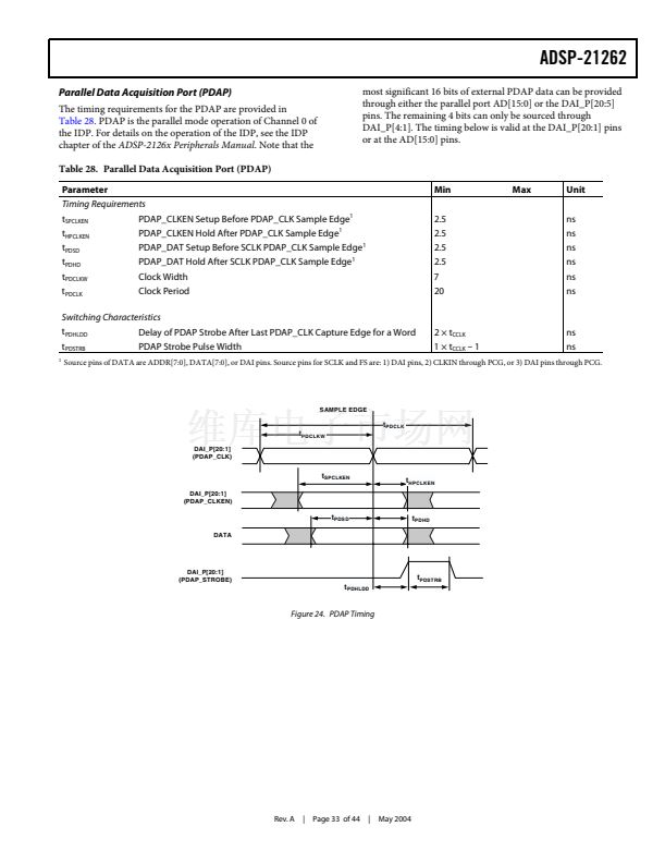
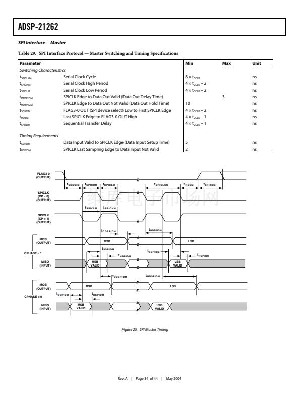
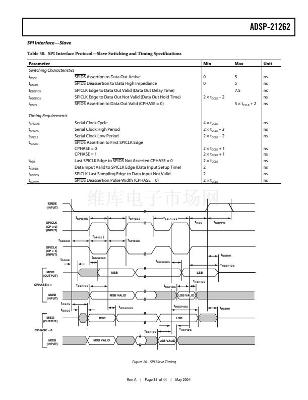
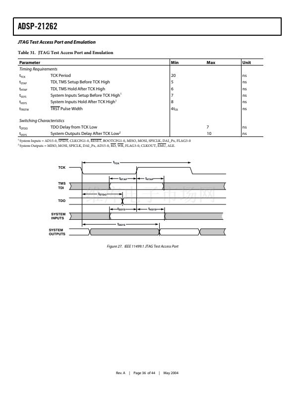
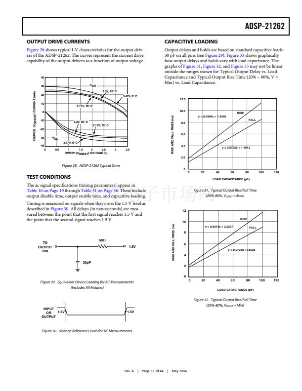
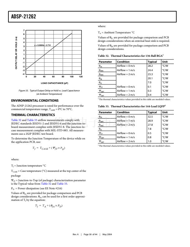
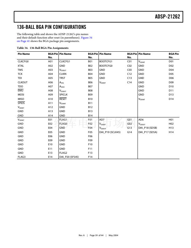
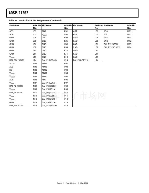
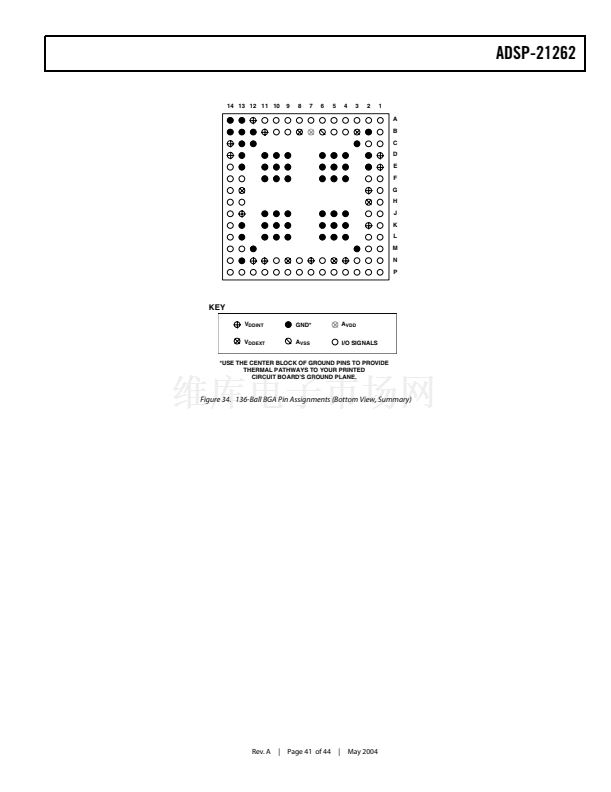
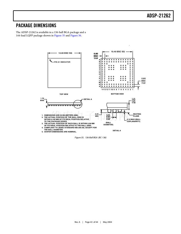
ADSP-21262
ABSOLUTE MAXIMUM RATINGS
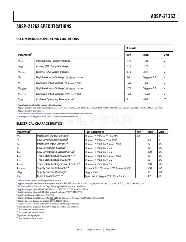
Parameter
Internal (Core) Supply Voltage (V
DDINT
)
1
Analog (PLL) Supply Voltage (A
VDD
)
1
External (I/O) Supply Voltage (V
DDEXT
)
1
Input Voltage鈥?.5 V to V
DDEXT1
Output Voltage Swing鈥?.5 V to V
DDEXT1
Load Capacitance
1
Storage Temperature Range
1
Junction Temperature under Bias
1
Rating
鈥?.3 V to +1.4 V
鈥?.3 V to +1.4 V
鈥?.3 V to +3.8 V
+ 0.5 V
+ 0.5 V
200 pF
鈥?5掳C to +150掳C
125掳C
Stresses greater than those listed above may cause permanent damage to the device. These are stress ratings only;
functional operation of the device at these or any other conditions greater than those indicated in the operational
sections of this specification is not implied. Exposure to absolute maximum rating conditions for extended periods
may affect device reliability.
ESD SENSITIVITY
CAUTION
ESD (electrostatic discharge) sensitive device. Electrostatic charges as high as 4000 V readily
accumulate on the human body and test equipment and can discharge without detection.
Although the ADSP-21262 features proprietary ESD protection circuitry, permanent
damage may occur on devices subjected to high energy electrostatic discharges. Therefore,
proper ESD precautions are recommended to avoid performance degradation or loss of
functionality.
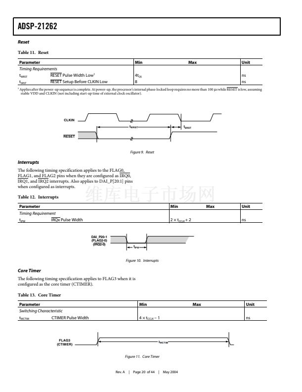
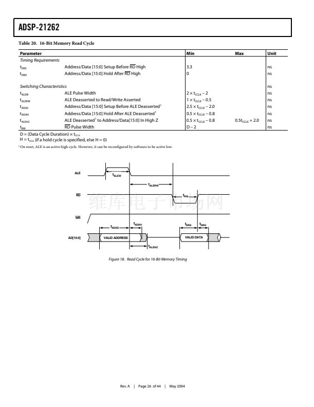
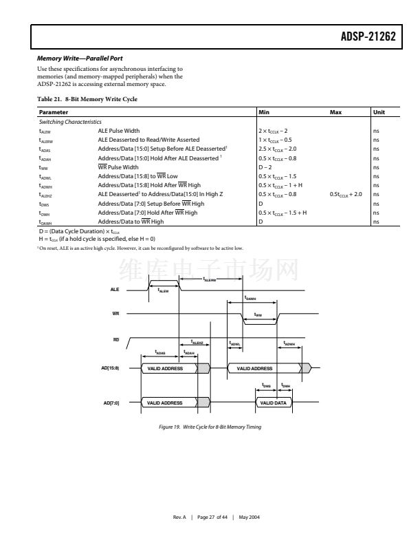
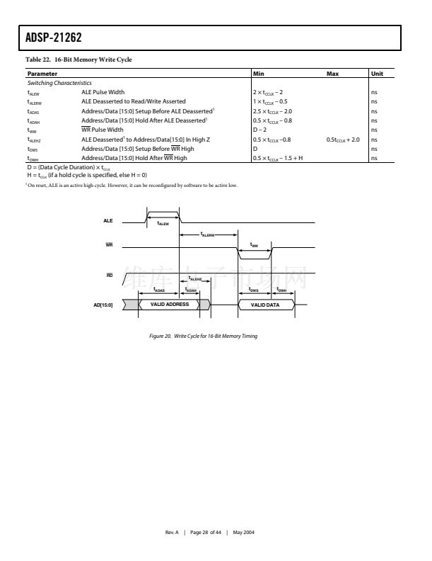
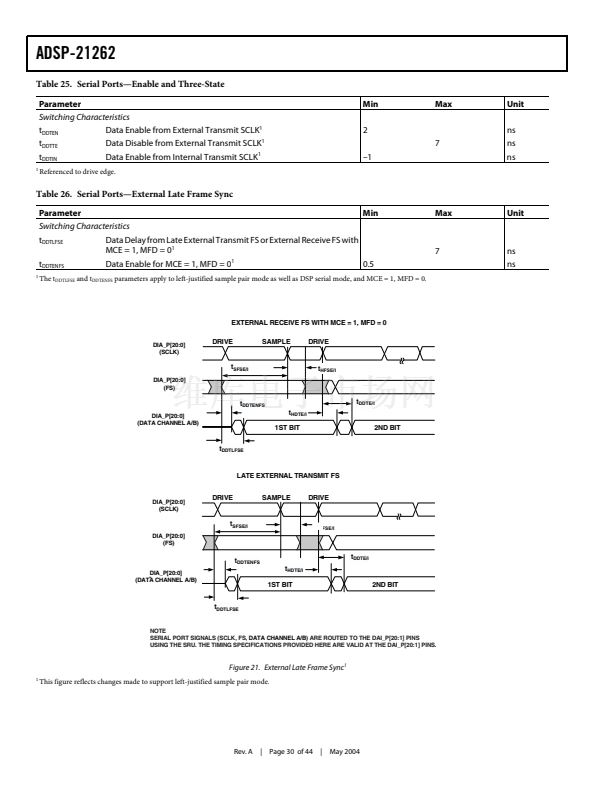
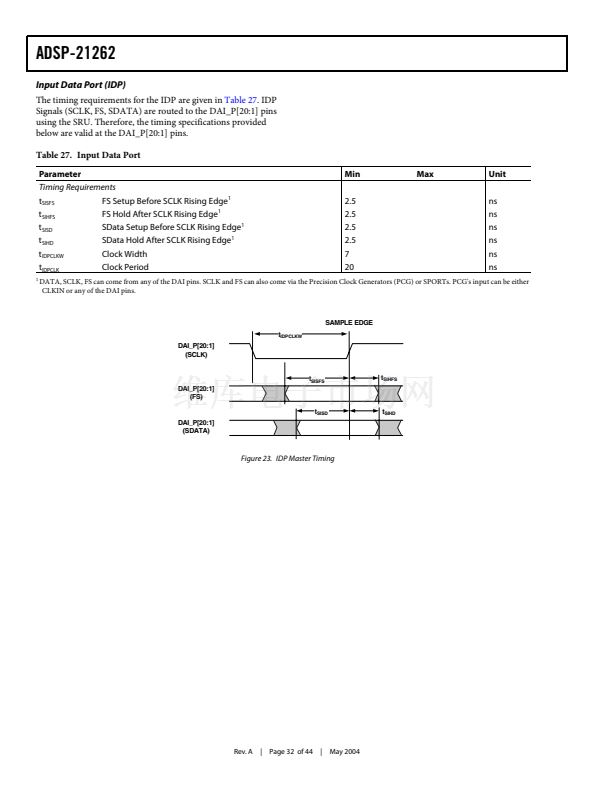
TIMING SPECIFICATIONS
The ADSP-21262鈥檚 internal clock (a multiple of CLKIN) pro-
vides the clock signal for timing internal memory, processor
core, serial ports, and parallel port (as required for read/write
strobes in asynchronous access mode). During reset, program
the ratio between the DSP鈥檚 internal clock frequency and exter-
nal (CLKIN) clock frequency with the CLKCFG1-0 pins. To
determine switching frequencies for the serial ports, divide
down the internal clock, using the programmable divider con-
trol of each port (DIVx for the serial ports).
The ADSP-21262鈥檚 internal clock switches at higher frequencies
than the system input clock (CLKIN). To generate the internal
clock, the DSP uses an internal phase-locked loop (PLL). This
PLL-based clocking minimizes the skew between the system
clock (CLKIN) signal and the DSP鈥檚 internal clock (the clock
source for the parallel port logic and I/O pads).
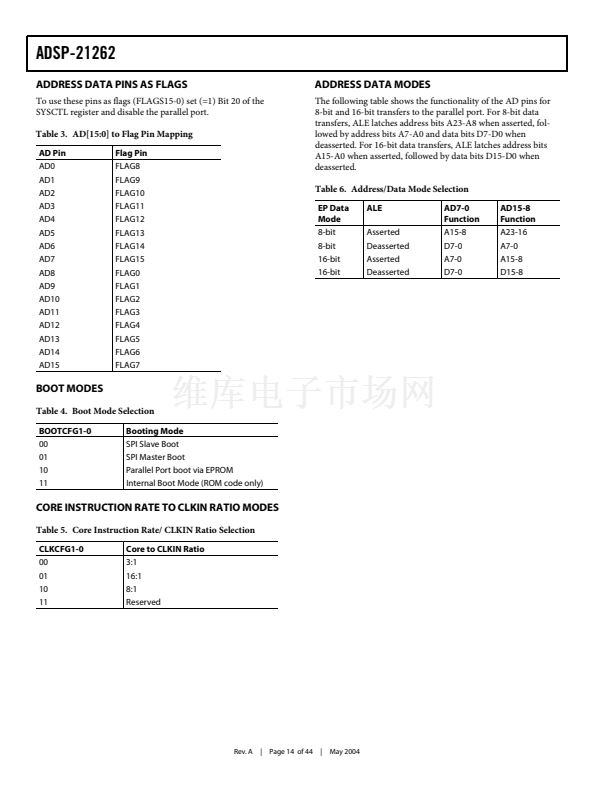
Note the definitions of various clock periods that are a function
of CLKIN and the appropriate ratio control (Table
7
and
Table 8).
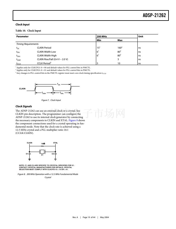
Table 7. ADSP-21262 CLKOUT and CCLK Clock
Generation Operation
Timing
Requirements
CLKIN
CCLK
Description
Input Clock
Core Clock
Calculation
1/t
CK
1/t
CCLK
Table 8. Clock Periods
Timing
Requirements
t
CK
t
CCLK
t
SCLK
t
SPICLK
1
Description
1
CLKIN Clock Period
(Processor) Core Clock Period
Serial Port Clock Period = (t
CCLK
) 脳 SR
SPI Clock Period = (t
CCLK
) 脳 SPIR
where:
SR = serial port-to-core clock ratio (wide range, determined by
SPORT CLKDIV)
SPIR = SPI-to-Core Clock Ratio (wide range, determined by
SPIBAUD register)
DAI_Px = Serial Port Clock
SPICLK = SPI Clock
Figure 5
shows Core to CLKIN ratios of 3:1, 8:1, and 16:1 with
external oscillator or crystal. Note that more ratios are possible
and can be set through software using the power management
control register (PMCTL). For more information, see the
ADSP-2126x SHARC DSP Core Manual.
Use the exact timing information given. Do not attempt to
derive parameters from the addition or subtraction of others.
While addition or subtraction would yield meaningful results
for an individual device, the values given in this data sheet
reflect statistical variations and worst cases. Consequently, it is
not meaningful to add parameters to derive longer times.
See
Figure 30 on Page 37
under Test conditions for voltage ref-
erence levels.
Rev. A |
Page 16 of 44 |
May 2004


 1
1
 2
2
 3
3
 4
4
 5
5
 6
6
 7
7
 8
8
 9
9
 10
10
 11
11
 12
12
 13
13
 14
14
 15
15
 16
16
 17
17
 18
18
 19
19
 20
20
 21
21
 22
22
 23
23
 24
24
 25
25
 26
26
 27
27
 28
28
 29
29
 30
30
 31
31
 32
32
 33
33
 34
34
 35
35
 36
36
 37
37
 38
38
 39
39
 40
40
 41
41
 42
42
 43
43
 44
44
