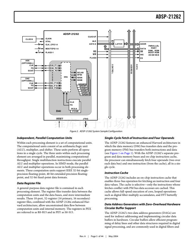
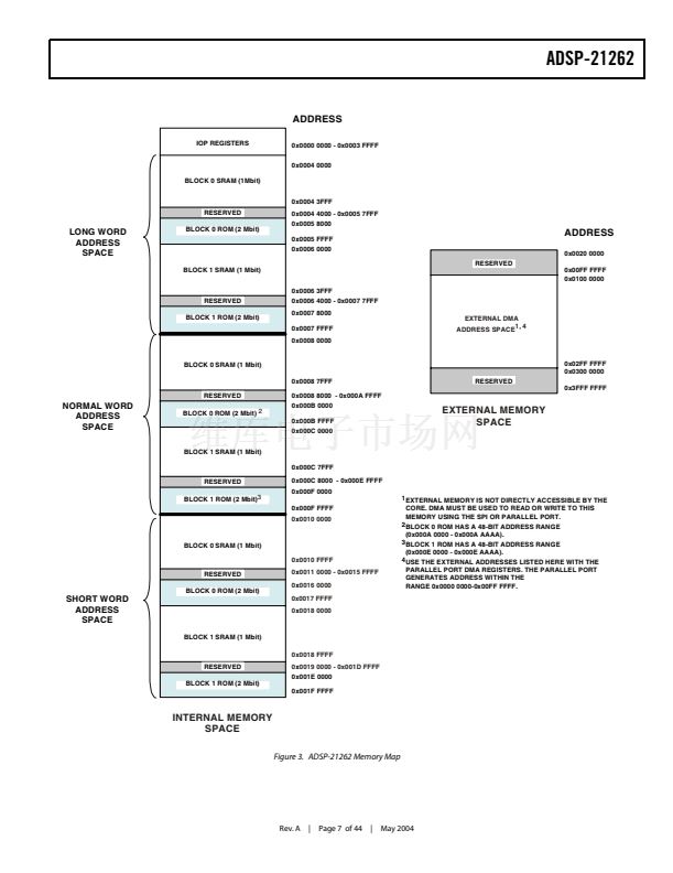
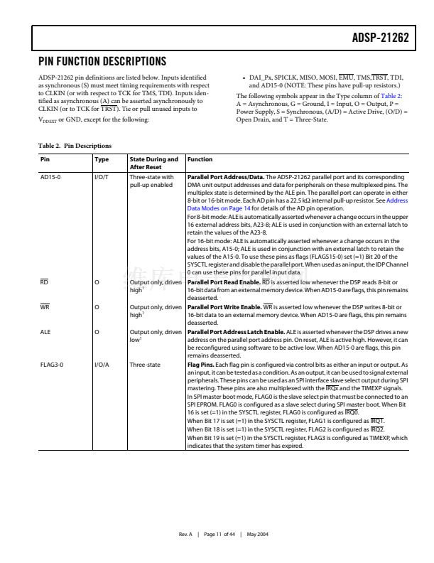
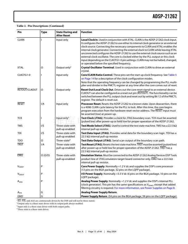
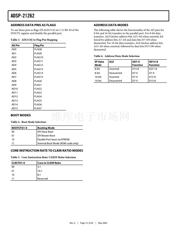
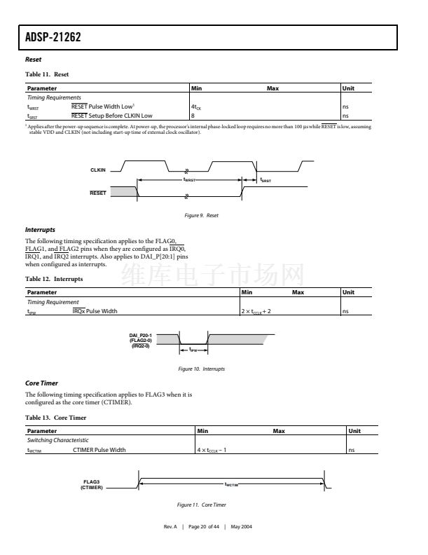
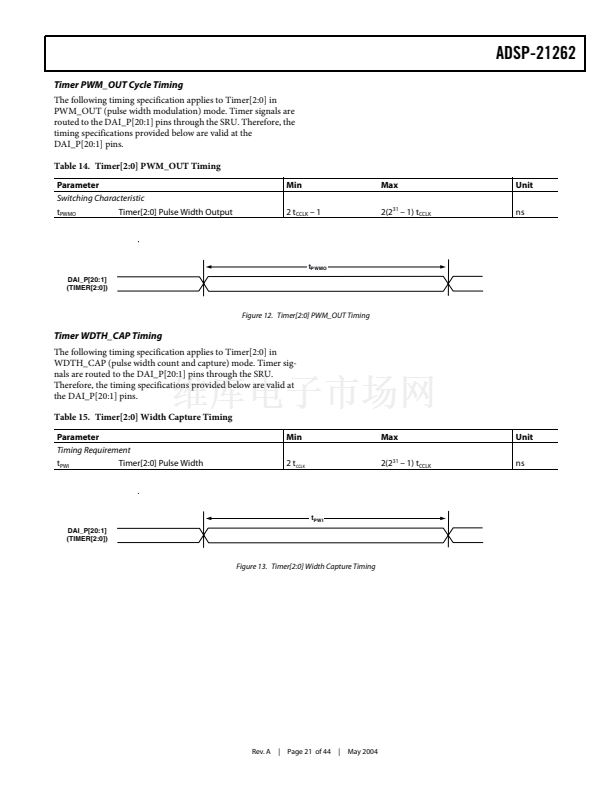
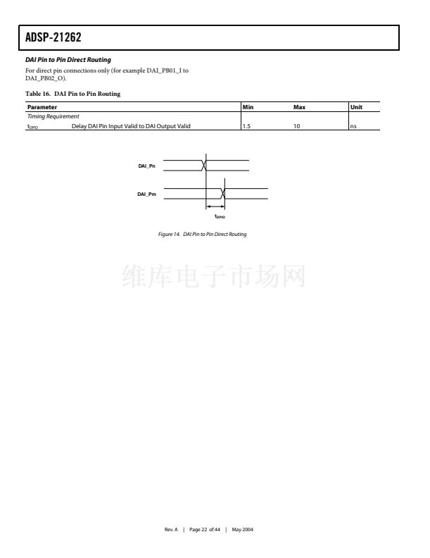
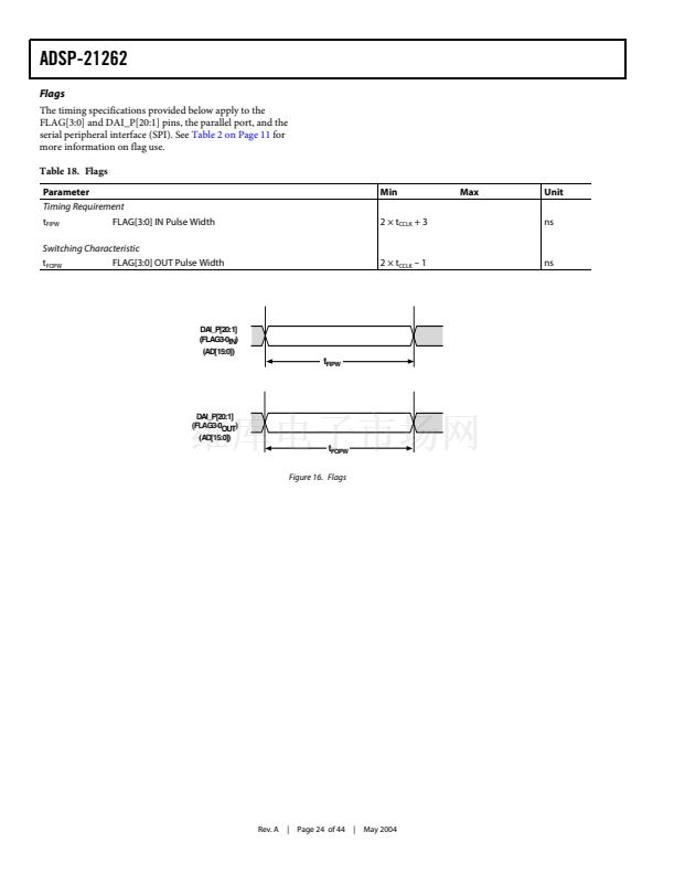
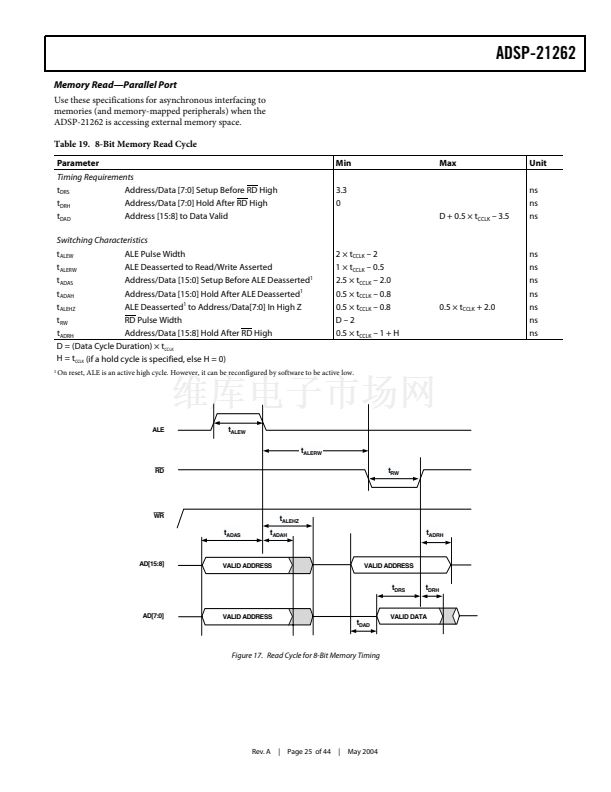
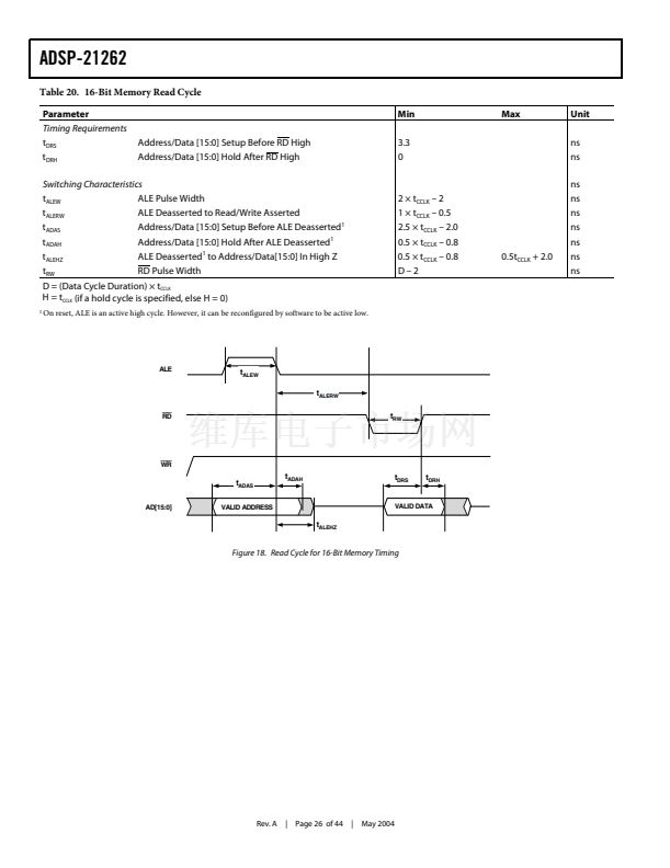
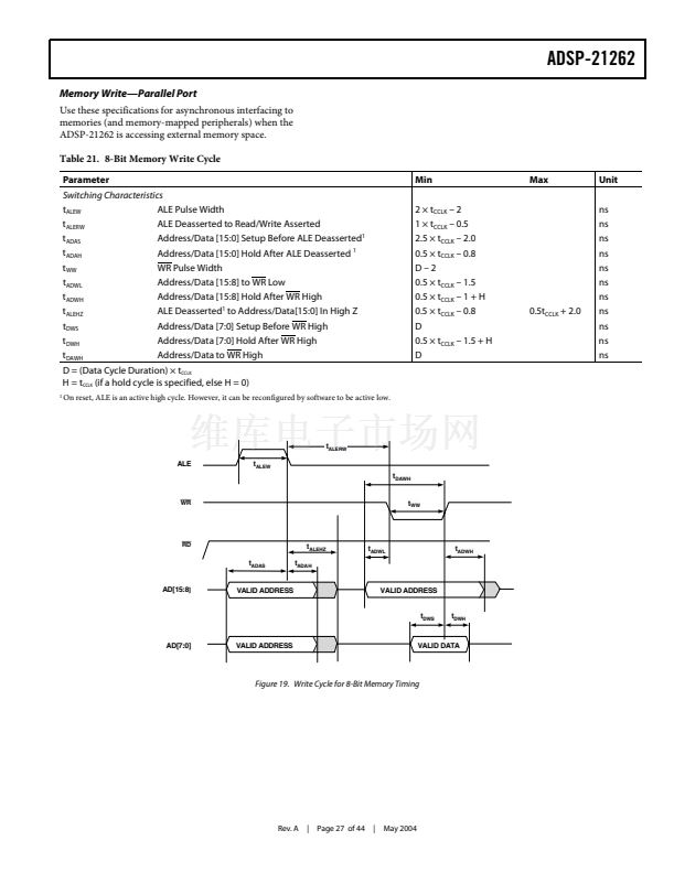
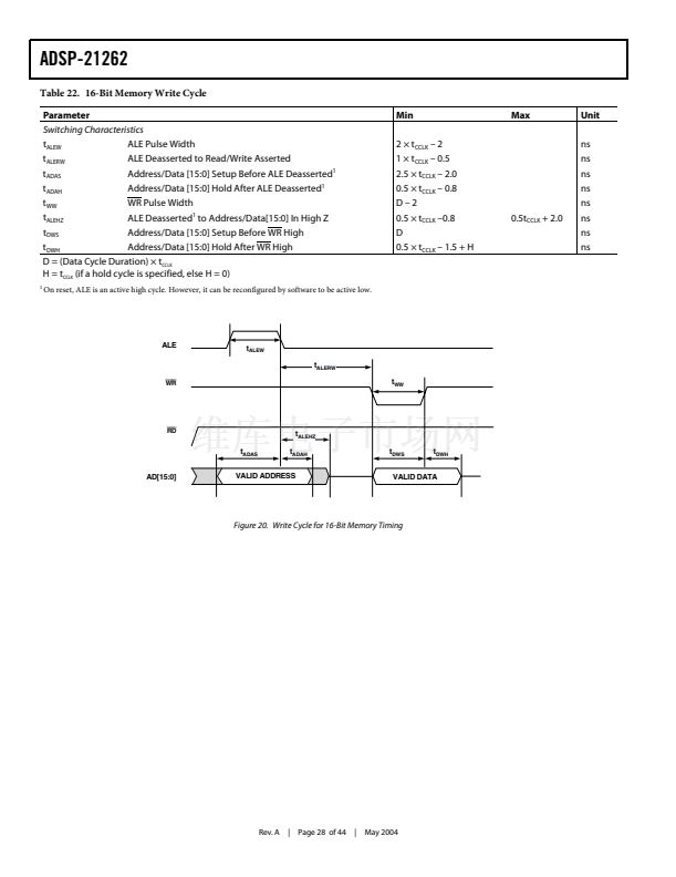
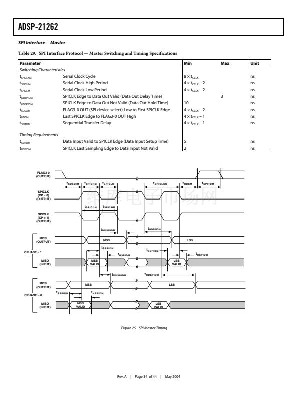
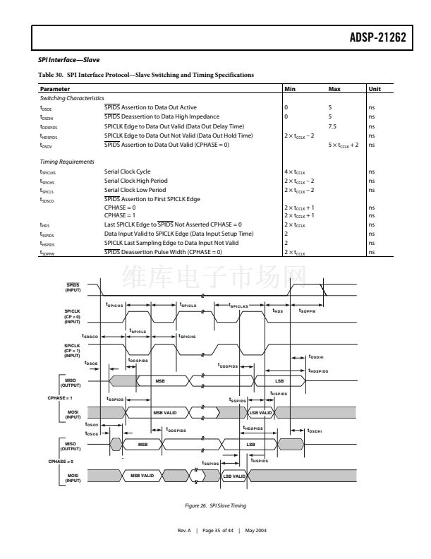
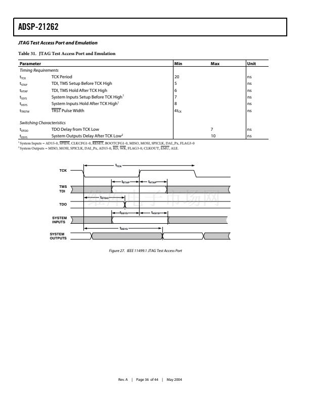
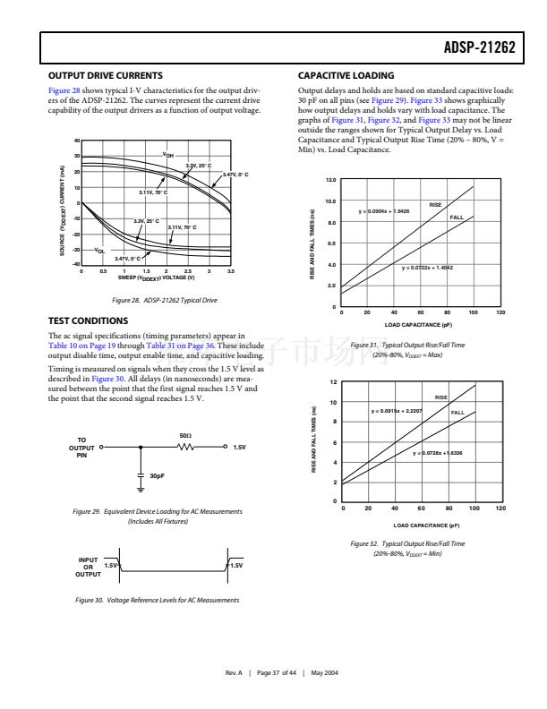
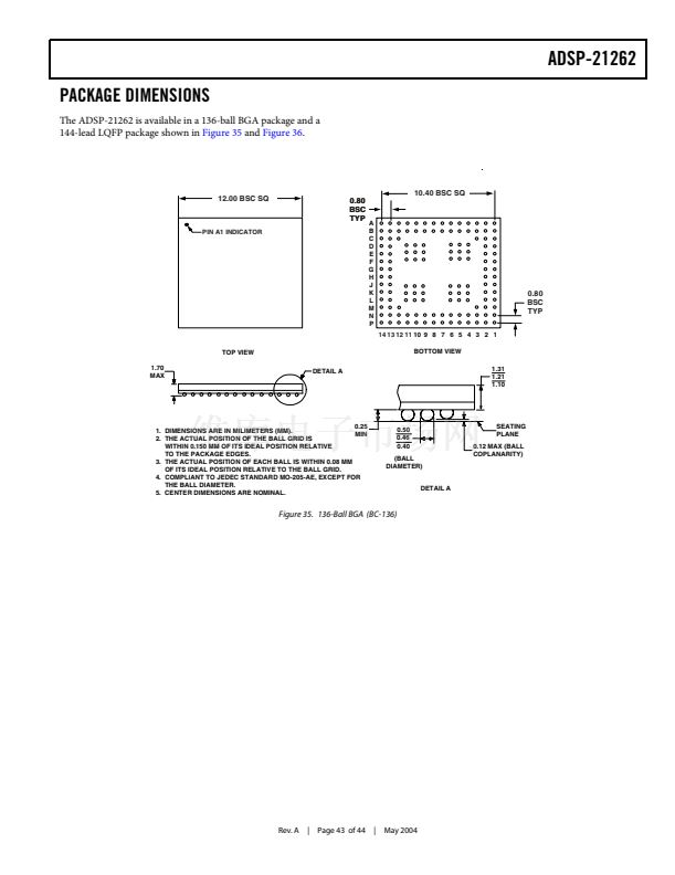
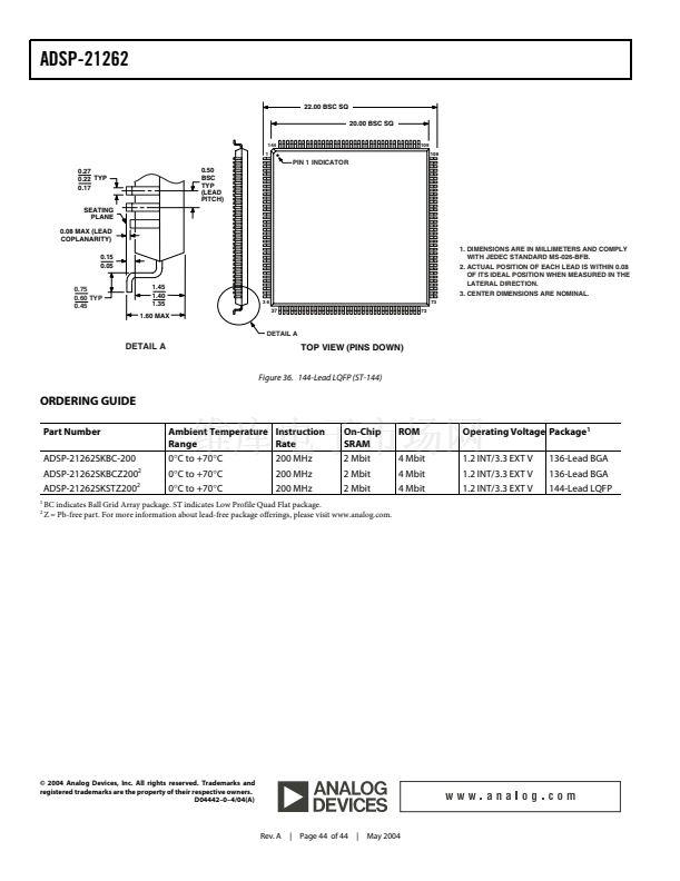
ADSP-21262
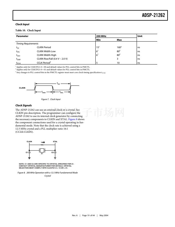
Clock Input
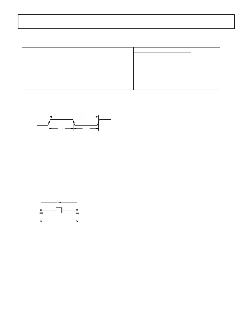
Table 10. Clock Input
Parameter
Timing Requirements
t
CK
CLKIN Period
t
CKL
CLKIN Width Low
t
CKH
CLKIN Width High
t
CKRF
CLKIN Rise/Fall (0.4 V 鈥?2.0 V)
t
CCLK
CCLK Period
3
1
2
200 MHz
Min
15
1
6
1
6
1
5
Unit
Max
160
2
80
2
80
2
3
10
ns
ns
ns
ns
ns
Applies only for CLKCFG1-0 = 00 and default values for PLL control bits in PMCTL.
Applies only for CLKCFG1-0 = 01 and default values for PLL control bits in PMCTL.
3
Any changes to PLL control bits in the PMCTL register must meet core clock timing specification t
CCLK
.
t
CK
CLKIN
t
CKH
t
CKL
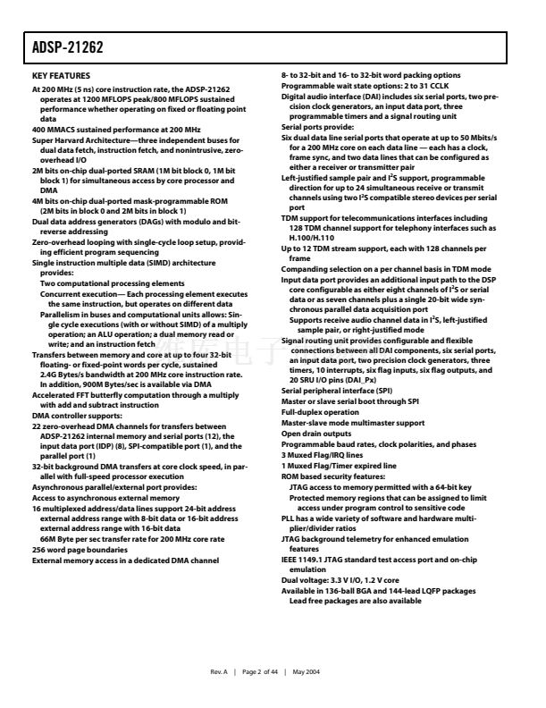
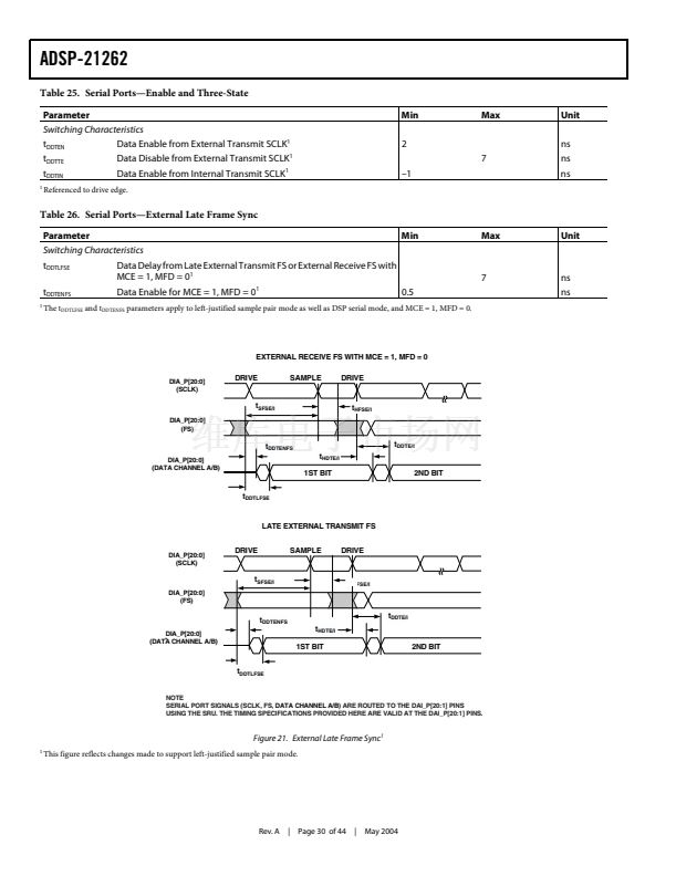
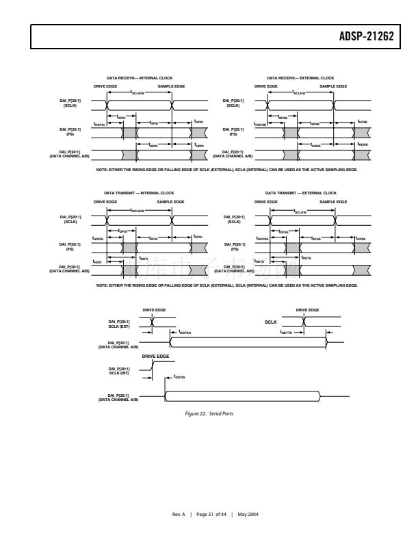
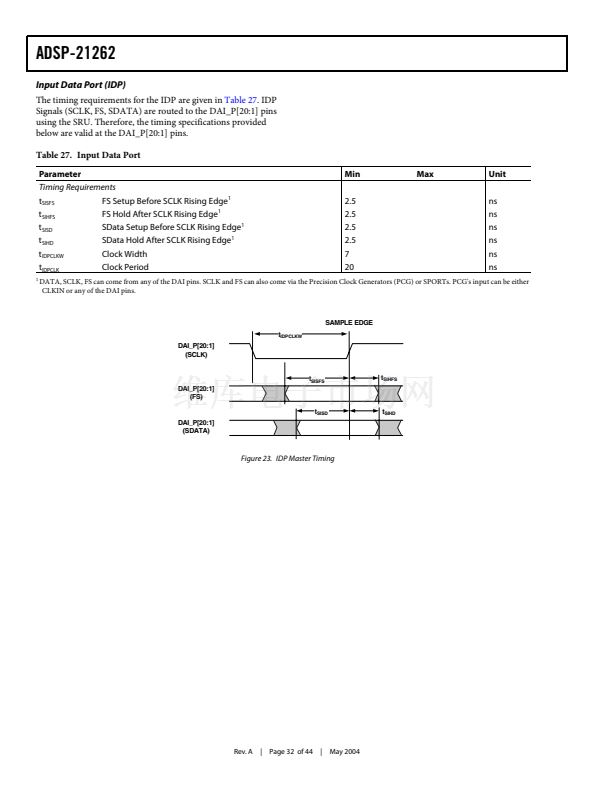
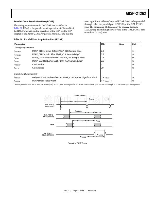
Figure 7. Clock Input
Clock Signals
The ADSP-21262 can use an external clock or a crystal. See
CLKIN pin description. The programmer can configure the
ADSP-21262 to use its internal clock generator by connecting
the necessary components to CLKIN and XTAL.
Figure 8
shows
the component connections used for a crystal operating in fun-
damental mode. Note that the clock rate is achieved using a
12.5 MHz crystal and a PLL multiplier ratio 16:1
(CCLK:CLKIN).
CLKIN
1M
XTAL
C1
X1
C2
NOTE: C1 AND C2 ARE SPECIFIC TO CRYSTAL SPECIFIED FOR X1.
CONTACT CRYSTAL MANUFACTURER FOR DETAILS. CRYSTAL
SELECTION MUST COMPLY WITH CLKCFG1-0 = 10 OR = 01.
Figure 8. 200 MHz Operation with a 12.5 MHz Fundamental Mode
Crystal
Rev. A |
Page 19 of 44 |
May 2004


 1
1
 2
2
 3
3
 4
4
 5
5
 6
6
 7
7
 8
8
 9
9
 10
10
 11
11
 12
12
 13
13
 14
14
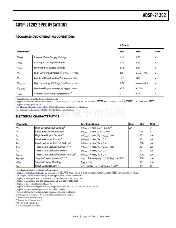 15
15
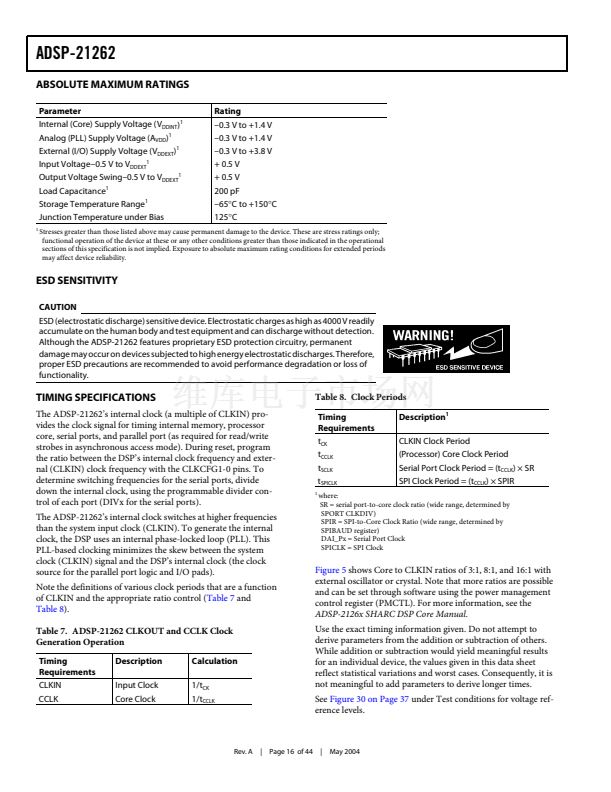 16
16
 17
17
 18
18
 19
19
 20
20
 21
21
 22
22
 23
23
 24
24
 25
25
 26
26
 27
27
 28
28
 29
29
 30
30
 31
31
 32
32
 33
33
 34
34
 35
35
 36
36
 37
37
 38
38
 39
39
 40
40
 41
41
 42
42
 43
43
 44
44
